CXA1875AP データシートの表示(PDF) - Sony Semiconductor
部品番号
コンポーネント説明
メーカー
CXA1875AP Datasheet PDF : 10 Pages
| |||
CXA1875AP/AM
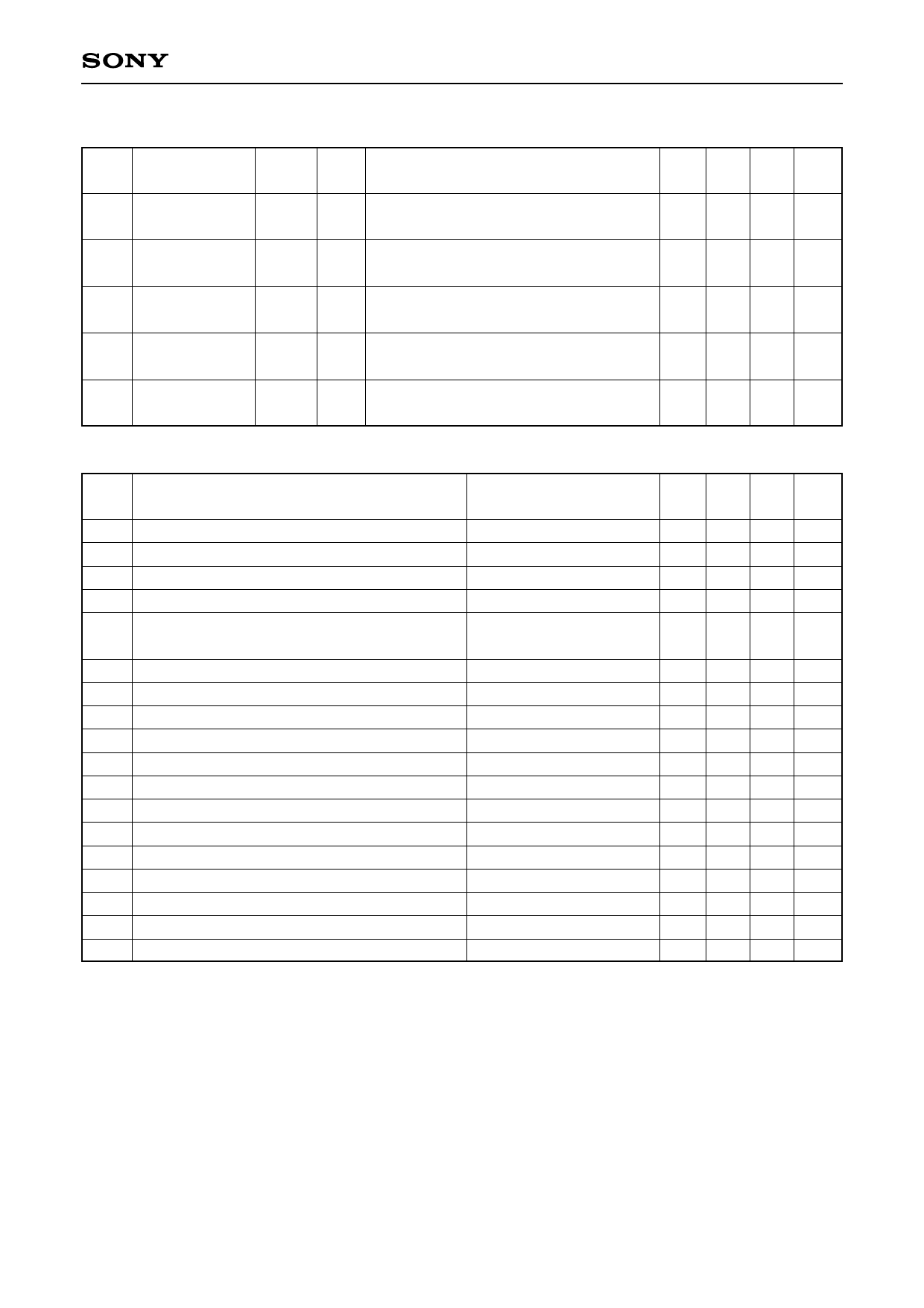
SW, SAD Pins
Text
No.
Item
Symbol
circuit
Test contents
Min. Typ. Max. Unit
Low level input
7
VIL
voltage
3 ST 0 to 3 an input voltage that turns to ‘0’ — — 1.5 V
High level input
8
VIH
voltage
3 ST 0 to 3 an input voltage that turns to ‘1’ 3.0 — — V
Low level input
9
IIL
current
3 Input current when 0.4 V is applied
–10 0 +10 µA
High level input
10
IIH
current
3 Input current when 4.5 V is applied
–10 0 +10 µA
Low level input
11
VOL
voltage
SW 0 to 3=1, Output voltage when 1 mA
4
0 0.2 0.4 V
flows in
I2C Bus Block Items (SDA, SCL)
No.
Item
12 High level input voltage
13 Low level input voltage
14 High level input current
15 Low level input current
Low level output voltage
16
At 3 mA flow to SDA (Pin 14)
17 Maximum flowing current
18 Input capacitance
19 Maximum clock frequency
20 Data change minimum waiting time
21 Data transfer start minimum waiting time
22 Low level clock pulse width
23 High level clock pulse width
24 Minimum start preparation waiting time
25 Minimum data hold time
26 Minimum data preparation time
27 Rise time
28 Fall time
29 Minimum stop preparation waiting time
Symbol
VIH
VIL
IIH
IIL
VOL
IOL
CI
fSCL
tBUF
tHD:STA
tLOW
tHIGH
tSU:STA
tHD:DAT
tSU:DAT
tR
tF
tSU:STO
Min. Typ. Max. Unit
3.0 — 5.0 V
0 — 1.5 V
— — 10 µA
— — 10 µA
0 — 0.4 V
3 — — mA
— — 10 pF
0 — 100 kHz
4.7 — — µs
4.0 — — µs
4.7 — — µs
4.0 — — µs
4.7 — — µs
5 — — µs
250 — — ns
— — 1 µs
— — 300 ns
4.7 — — µs
I2C bus load conditions: Pull up resistance 4 kΩ (Connected to +5 V)
Load capacitance 200 pF (Connected to GND)
—4—
Share Link: 