PCF85102C-2T/03 гГЗгГЉгВњгВЈгГЉгГИгБЃи°®з§ЇпЉИPDFпЉЙ - Philips Electronics
йГ®еУБзХ™еПЈ
гВ≥гГ≥гГЭгГЉгГНгГ≥гГИи™ђжШО
гГ°гГЉгВЂгГЉ
PCF85102C-2T/03 Datasheet PDF : 20 Pages
| |||
Philips Semiconductors
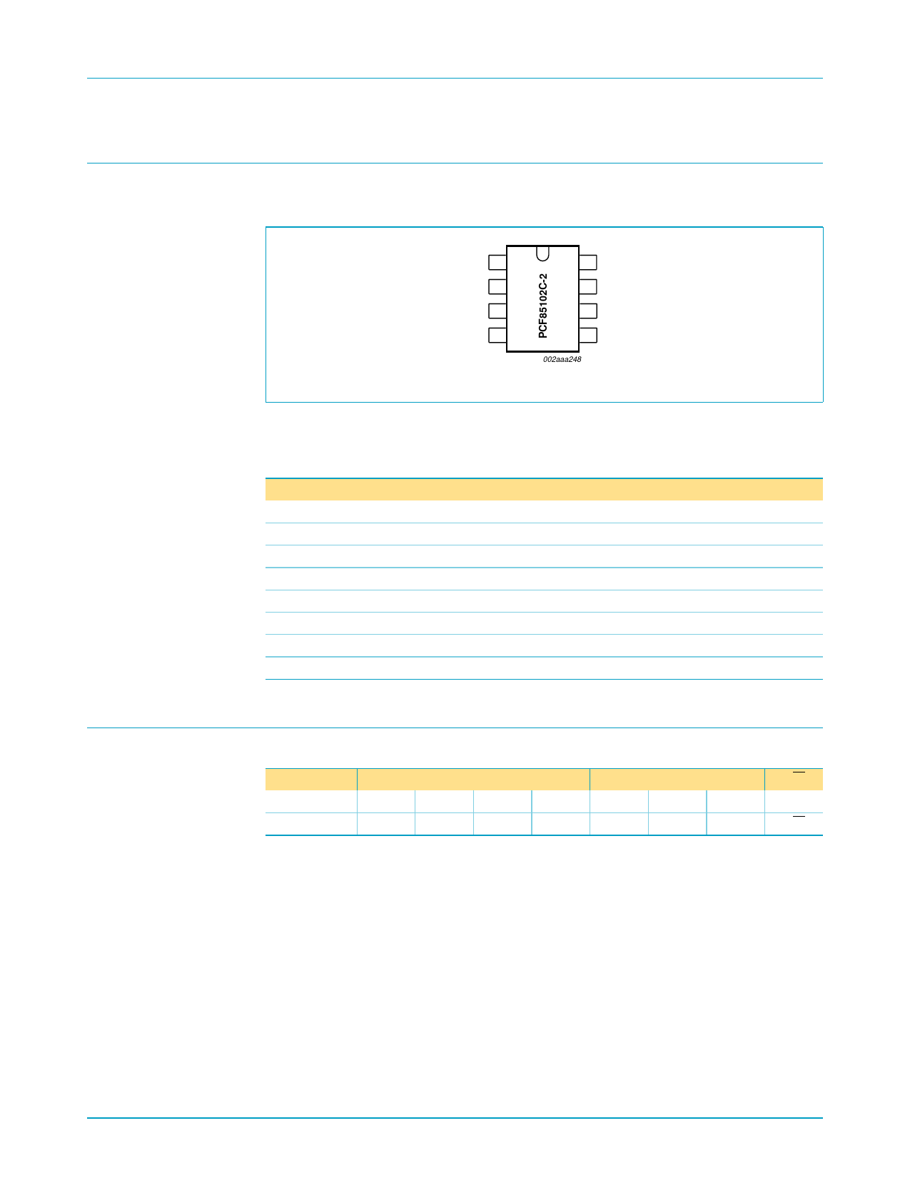
6. Pinning information
6.1 Pinning
PCF85102C-2
256 √Ч 8-bit CMOS EEPROM with I2C-bus interface
A0 1
A1 2
A2 3
VSS 4
Fig 2. Pin conпђБguration.
8 VDD
7 N.C.
6 SCL
5 SDA
002aaa248
6.2 Pin description
Table 4:
Symbol
A0
A1
A2
VSS
SDA
SCL
N.C.
VDD
Pin description
Pin
1
2
3
4
5
6
7
8
Description
address input 0
address input 1
address input 2
negative supply voltage
serial data input/output (I2C-bus)
serial clock input (I2C-bus)
no connect
positive supply voltage
7. Device addressing
Table 5: Device address code
Selection
Device code
Bit
b7[1]
b6
b5
b4
Device
1
0
1
0
[1] The Most SigniпђБcant Bit (MSB) вАШb7вАЩ is sent пђБrst.
Chip Enable
R/W
b3
b2
b1
b0
A2
A1
A0
R/W
A2, A1, A0 are hardware selectable pins.
A system could have up to eight PCF85102C-2 devices on the same I2C-bus,
equivalent to a 16 kbit EEPROM or 8 pages of 256 bytes of memory.
The eight addresses are deпђБned by the state of the A0, A1, A2 inputs (logic level вАШ1вАЩ
when connected to VDD, logic level вАШ0вАЩ when connected to GND). Figure 3 shows the
various address combinations.
9397 750 14216
Product data
Rev. 04 вАФ 22 October 2004
© Koninklijke Philips Electronics N.V. 2004. All rights reserved.
4 of 20
Share Link: 