PCF8532U/2DA/1 データシートの表示(PDF) - NXP Semiconductors.
部品番号
コンポーネント説明
メーカー
PCF8532U/2DA/1 Datasheet PDF : 44 Pages
| |||
NXP Semiconductors
PCF8532
Universal LCD driver for low multiplex rates
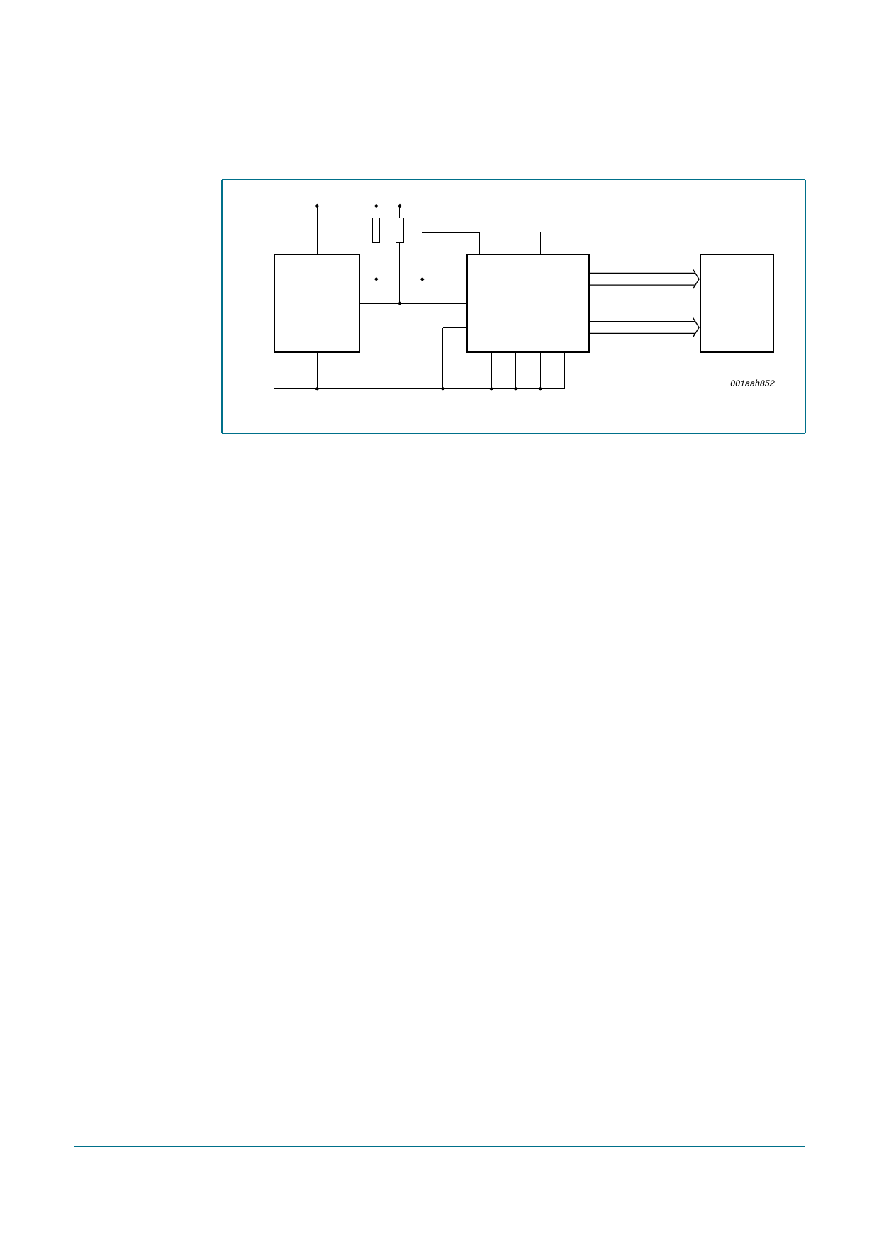
VDD
R
≤
tr
2CB
HOST
MICRO-
PROCESSOR/
MICRO-
CONTROLLER
SDAACK
SDA
SCL
OSC
VDD VLCD
160 segment drives
PCF8532
4 backplanes
LCD PANEL
(up to 640
elements)
A0 A1 SA0 VSS
VSS
001aah852
Fig 3. Typical system configuration
The host microprocessor or microcontroller maintains the 2-line I2C-bus communication
channel with the PCF8532.
Biasing voltages for the multiplexed LCD waveforms are generated internally, removing
the need for an external bias generator. The internal oscillator is selected by connecting
pin OSC to VSS. The only other connections required to complete the system are the
power supplies (VDD, VSS and VLCD) and the LCD panel selected for the application.
7.1 Power-on reset
At power-on the PCF8532 resets to a default starting condition:
• All backplane and segment outputs are set to VLCD
• The selected drive mode is 1:4 multiplex with 1⁄3 bias
• Blinking is switched off
• Input and output bank selectors are reset
• The I2C-bus interface is initialized
• The data pointer and the subaddress counter are cleared (set to logic 0)
• The display is disabled
• If internal oscillator is selected (OSC pin connected to VSS), then there is no clock
signal on pin CLK
Do not transfer data on the I2C-bus after a power-on for at least 1 ms to allow the reset
action to complete.
7.2 LCD bias generator
Fractional LCD biasing voltages are obtained from an internal voltage divider of three
series resistors connected between VLCD and VSS. The center resistor can be switched
out of the circuit to provide a 1⁄2 bias voltage level for the 1:2 multiplex configuration.
PCF8532_1
Product data sheet
Rev. 1 — 10 February 2009
© NXP B.V. 2009. All rights reserved.
5 of 44
Share Link: 