PCF8573 データシートの表示(PDF) - Philips Electronics
部品番号
コンポーネント説明
メーカー
PCF8573 Datasheet PDF : 28 Pages
| |||
Philips Semiconductors
Clock/calendar with serial I/O
Product specification
PCF8573
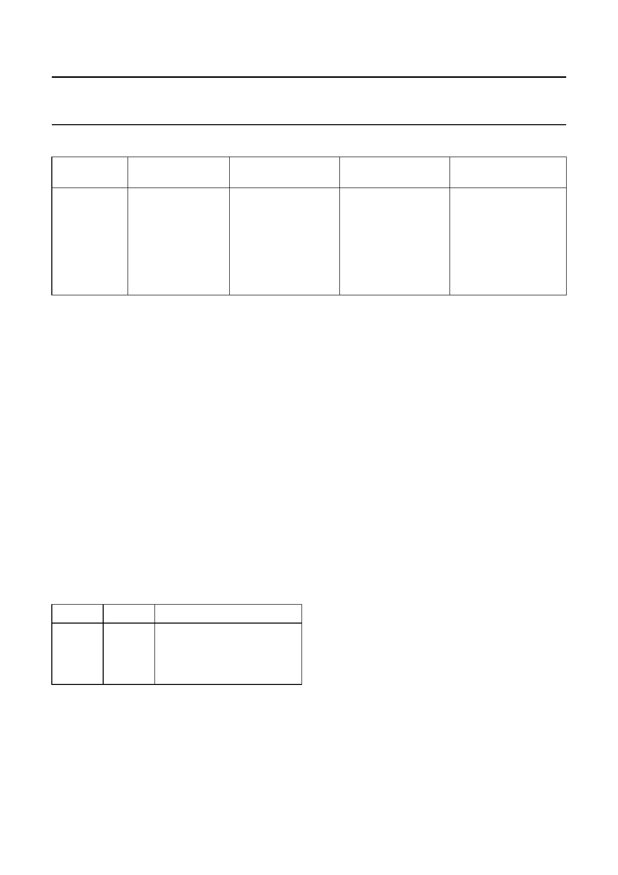
Table 1 Cycle length of the time counter
UNIT
minutes
hours
days(1)
months
NUMBER OF BITS COUNTING CYCLE
7
00 to 59
6
00 to 23
6
01 to 28
01 to 30
01 to 31
5
01 to 12
CARRY FOR
FOLLOWING UNIT
59 → 00
23 → 00
28 → 01
or 29 → 01
30 → 01
31 → 01
12 → 01
CONTENT OF MONTH
COUNTER
2
2
4, 6, 9, 11
1, 3, 5, 7, 8, 10, 12
Note
1. During February of a leap-year the ‘Time Counter Days’ may be set to 29 by directly writing to it using the ‘execute
address’ function. Leap-years must be tracked by the system software.
7.5 Power on/power fail detection
If the voltage VDD − VSS1 falls below a certain value, the
operation of the clock becomes undefined. Therefore a
warning signal is required to indicate that faultless
operation of the clock is not guaranteed. This information
is latched in a flag called POWF (Power Fail) and remains
latched after restoration of the correct supply voltage until
a write sequence with EXECUTE ADDRESS has been
received. The flag POWF can be set by an internally
generated power fail level-discriminator signal for
applications with (VDD − VSS1) greater than VTH1, or by an
externally generated power fail signal for applications with
(VDD − VSS1) less than VTH1. The external signal must be
applied to the input PFIN. The input stage operates with
signals of slow rise and fall times. Internally or externally
controlled POWF can be selected by input EXTPF as
shown in Table 2.
Table 2 Power fail selection
EXTPF(1) PFIN(1)
FUNCTION
0
0
power fail is sensed internally
0
1
test mode
1
0
power fail is sensed externally
1
1
no power fail sensed
Note
1. 0 = VSS1 (LOW); 1 = VDD (HIGH).
The external power fail control operates by absence of the
VDD − VSS2 supply. Therefore the input levels applied to
PFIN and EXTPF must be within the range VDD − VSS1.
A LOW level at PFIN indicates a power fail. POWF is
readable via the I2C-bus. A power-on reset for the I2C-bus
control is generated on-chip when the supply voltage
VDD − VSS2 is less than VTH2.
7.6 Interface level shifters
The level shifters adjust the 5 V operating voltage
(VDD − VSS2) of the microcontroller to the internal supply
voltage (VDD − VSS1) of the clock/calendar. The oscillator
and counter are not influenced by the VDD − VSS2 supply
voltage. If the voltage VDD − VSS2 is absent (VDD = VSS2),
the output signal of the level shifter is HIGH because VDD
is the common node of the VDD − VSS2 and VDD − VSS1
supplies. Because the level shifters invert the input
signals, the internal circuit behaves as if a LOW signal is
present on the inputs. FSET, SEC, MIN and COMP are
CMOS push-pull output stages. The driving capability of
these outputs is lost when the supply voltage
VDD − VSS2 = 0.
2003 Jan 27
6
Share Link: 