PE9313(2006) データシートの表示(PDF) - Peregrine Semiconductor Corp.
部品番号
コンポーネント説明
メーカー
PE9313
(Rev.:2006)
(Rev.:2006)
Peregrine Semiconductor Corp.

PE9313 Datasheet PDF : 7 Pages
| |||
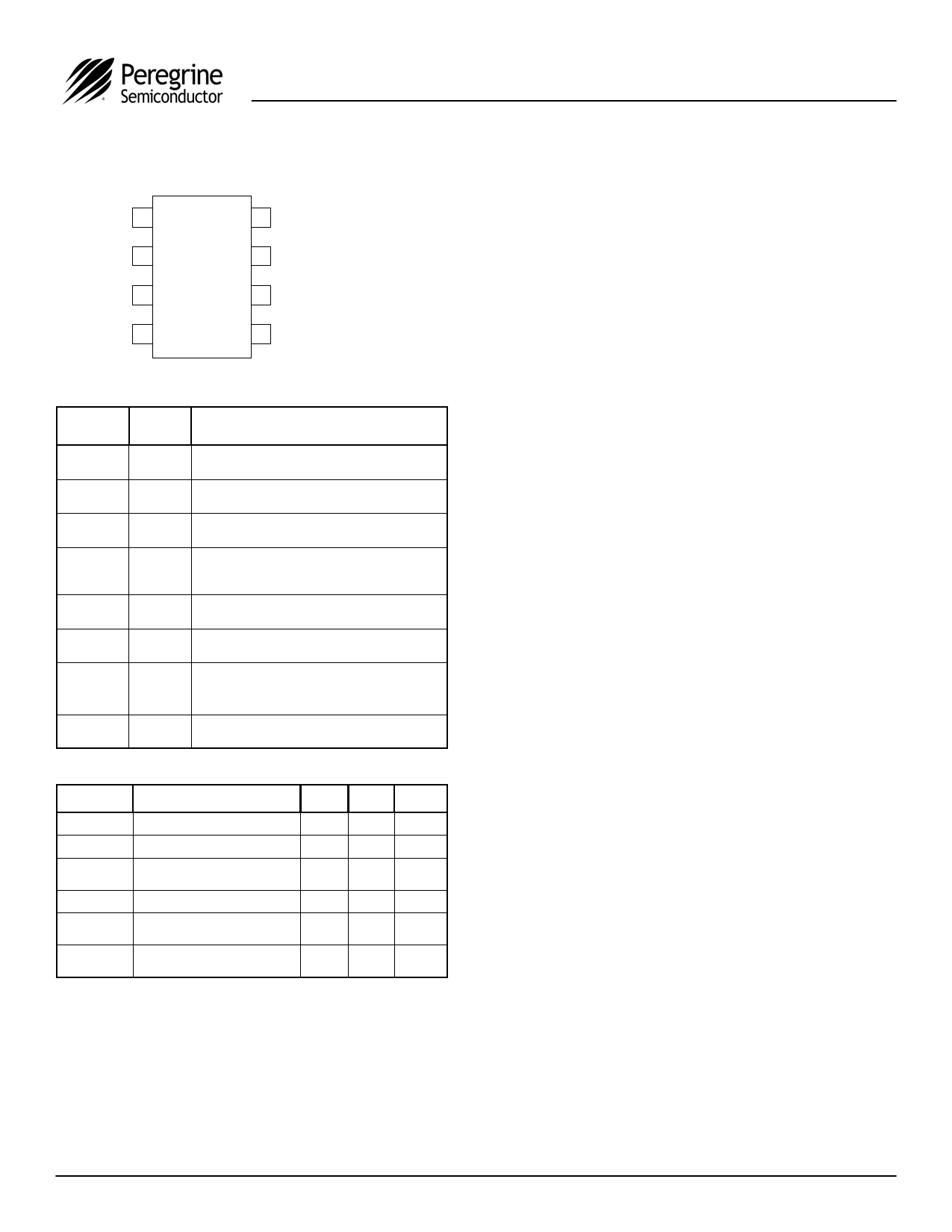
Figure 3. Pin Configuration
VDD
1
IN
2
N/C
3
GND 4
PE9313
8 GND
7 OUT
6 NC
5 GND
Table 2. Pin Descriptions
Pin No.
1
2
3
4
Pin
Name
VDD
IN
NC
GND
Description
Power supply pin. Bypassing is required
(eg 1000 pF & 100 pF).
Input signal pin. Should be coupled with a
capacitor (eg 1000 pF).
No connection. This pin should be left
open.
Ground pin. Ground pattern on the board
should be as wide as possible to reduce
ground impedance.
5
GND Ground pin.
6
NC
No connection. This pin should be left
open.
Divided frequency output pin. This pin
7
OUT should be coupled with a capacitor
(eg 1000 pF).
8
GND Ground Pin.
Table 3. Absolute Maximum Ratings
Symbol Parameter/Conditions Min Max Units
VDD Supply voltage
4.0
V
Pin
Input Power
15 dBm
VIN
Voltage on input
-0.3
VDD
+0.3
V
TST Storage temperature range
-65 150
°C
TOP
Operating temperature range -40
85
°C
VESD
ESD voltage (Human Body
Model, MIL-STD 883)
1000
V
Absolute Maximum Ratings are those values
listed in the above table. Exceeding these values
may cause permanent device damage.
PE9313
Product Specification
Electrostatic Discharge (ESD) Precautions
When handling this UltraCMOS™ device, observe
the same precautions that you would use with
other ESD-sensitive devices. Although this device
contains circuitry to protect it from damage due to
ESD, precautions should be taken to avoid
exceeding the rating specified in Table 3.
Latch-Up Avoidance
Unlike conventional CMOS devices, UltraCMOS™
devices are immune to latch-up.
Device Functional Considerations
The PE9313 divides an input signal, up to a
frequency of 1500 MHz, by a factor of eight
thereby producing an output frequency at an
eighth of the input frequency. To work properly at
higher frequency, the input and output signals
(pins 2 & 7) must be AC coupled via an external
capacitor, as shown in the test circuit in Figure 7.
The input may be DC coupled for low frequency
operation with care taken to remain within the
specified DC input range for the device.
The ground pattern on the board should be made
as wide as possible to minimize ground
impedance. See Figure 8 for a layout example.
©2003-2006 Peregrine Semiconductor Corp. All rights reserved.
Page 2 of 7
Document No. 70-0120-03 │ UltraCMOS™ RFIC Solutions
Share Link: