SN74LS165 データシートの表示(PDF) - Motorola => Freescale
部品番号
コンポーネント説明
メーカー
SN74LS165 Datasheet PDF : 6 Pages
| |||
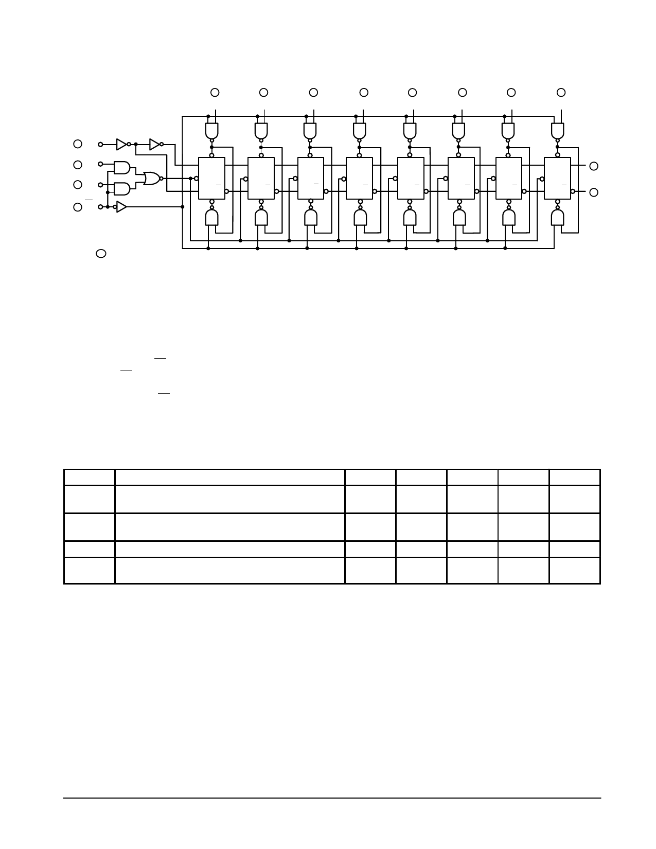
LOGIC DIAGRAM
10 DS
2 CP1
15 CP2
1 PL
VCC = PIN 16
GND = PIN 8
= PIN NUMBERS
SN54 / 74LS165
11
12
13
14
3
4
5
6
P0
P1
P2
P3
P4
P5
P6
P7
PRESET
S Q0
CP
R CLQ0
PRESET
S Q1
CP
R CLQ1
PRESET
S Q2
CP
R CLQ2
PRESET
S Q3
CP
R CLQ3
PRESET
S Q4
CP
R CLQ4
PRESET
S Q5
CP
R CLQ5
PRESET
S Q6
CP
R CLQ6
PRESET
S Q7
9
CP
R CLQ7
7
FUNCTIONAL DESCRIPTION
The SN54/74LS165 contains eight clocked master/slave
RS flip-flops connected as a shift register, with auxiliary gating
to provide overriding asynchronous parallel entry. Parallel
data enters when the PL signal is LOW. The parallel data can
change while PL is LOW, provided that the recommended set-
up and hold times are observed.
For clock operation, PL must be HIGH. The two clock inputs
perform identically; one can be used as a clock inhibit by
applying a HIGH signal. To avoid double clocking, however,
the inhibit signal should only go HIGH while the clock is HIGH.
Otherwise, the rising inhibit signal will cause the same
response as a rising clock edge. The flip-flops are
edge-triggered for serial operations. The serial input data can
change at any time, provided only that the recommended
setup and hold times are observed, with respect to the rising
edge of the clock.
GUARANTEED OPERATING RANGES
Symbol
Parameter
VCC
Supply Voltage
TA
Operating Ambient Temperature Range
IOH
Output Current — High
IOL
Output Current — Low
Min
Typ
Max
Unit
54
4.5
5.0
5.5
V
74
4.75
5.0
5.25
54
– 55
25
125
°C
74
0
25
70
54, 74
– 0.4
mA
54
4.0
mA
74
8.0
FAST AND LS TTL DATA
5-291
Share Link: 