HT48CA3(2003) データシートの表示(PDF) - Holtek Semiconductor
部品番号
コンポーネント説明
メーカー
HT48CA3 Datasheet PDF : 36 Pages
| |||
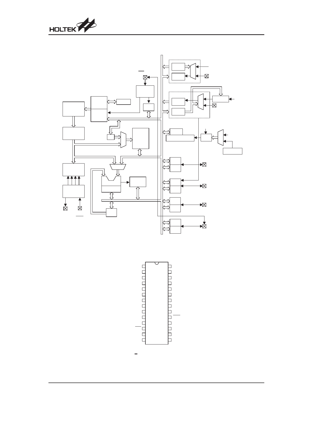
Pin Assignment
PB5 1
PB4 2
PA3 3
PA2 4
PA1 5
PA0 6
PB3 7
PB2 8
PB1 9
P B 0 /P F D 1 0
V S S 11
P F 0 /IN T 1 2
P C 0 /T M R 0 1 3
P C 1 14
28 P B 6
27 P B 7
26 P A 4
25 P A 5
24 P A 6
23 P A 7
22 O S C 2
21 O S C 1
20 V D D
19 R E S
1 8 P C 5 /T M R 1
17 P C 4
16 P C 3
15 P C 2
H T48C A 3
2 8 S K D IP -A /S O P -A
HT48CA3
Pin Description
Pin Name I/O
RES
I
PA0~PA7
I/O
PB0/PFD
PB1~PB7
I/O
VSS
¾
PC0/TMR0
PC1~PC4
I/O
PC5/TMR1
PF0/INT
I/O
VDD
¾
OSC1
I
OSC2
O
Note:
* Bit option
** Nibble option
*** Byte option
ROM Code
Option
¾
Wake-up*
Pull-high***
Pull-high**
PB0 or PFD
¾
Pull-high*
Pull-high*
¾
Crystal
or RC
Description
Schmitt trigger reset input, active low.
Bidirectional 8-bit input/output port. Each bit can be configured as a
wake-up input by a mask option. Software instructions determine the
CMOS output or Schmitt trigger input with/without pull-high resistor. The
pull-high resistor of each input/output line is also optional.
Bidirectional 8-bit input/output port. Software instructions determine
the CMOS output or Schmitt trigger input with/without pull-high resis-
tor. The pull-high resistor of each input/output line is also optional. The
output mode of PB0 can be used as an internal PFD signal output and
it can be used as a various frequency carrier signal.
Negative power supply, ground
Bidirectional 6-bit input/output port. Software instructions determine
the CMOS output or Schmitt trigger input with/without pull-high resis-
tor. The pull-high resistor of each input/output line is also optional. PC0
and PC5 are pin shared with TMR0 and TMR1 function pins.
Bidirectional 1-bit input/output port. Software instructions determine
the CMOS output or Schmitt trigger input with/without pull-high resis-
tor. The pull-high resistor of this input/output line is also optional. PF0
is pin shared with the INT function pin.
Positive power supply
OSC1, OSC2 are connected to an RC network or Crystal (determined
by hardware option) for the internal system clock. In the case of RC op-
eration, OSC2 is the output terminal for 1/4 system clock.
Rev. 1.40
2
July 16, 2003
Share Link: 