HT48CA3(2003) データシートの表示(PDF) - Holtek Semiconductor
部品番号
コンポーネント説明
メーカー
HT48CA3 Datasheet PDF : 36 Pages
| |||
HT48CA3
Absolute Maximum Ratings
Supply Voltage ...........................VSS-0.3V to VSS+4.0V
Input Voltage..............................VSS-0.3V to VDD+0.3V
Storage Temperature ............................-50°C to 125°C
Operating Temperature...........................-40°C to 85°C
Note: These are stress ratings only. Stresses exceeding the range specified under ²Absolute Maximum Ratings² may
cause substantial damage to the device. Functional operation of this device at other conditions beyond those
listed in the specification is not implied and prolonged exposure to extreme conditions may affect device reliabil-
ity.
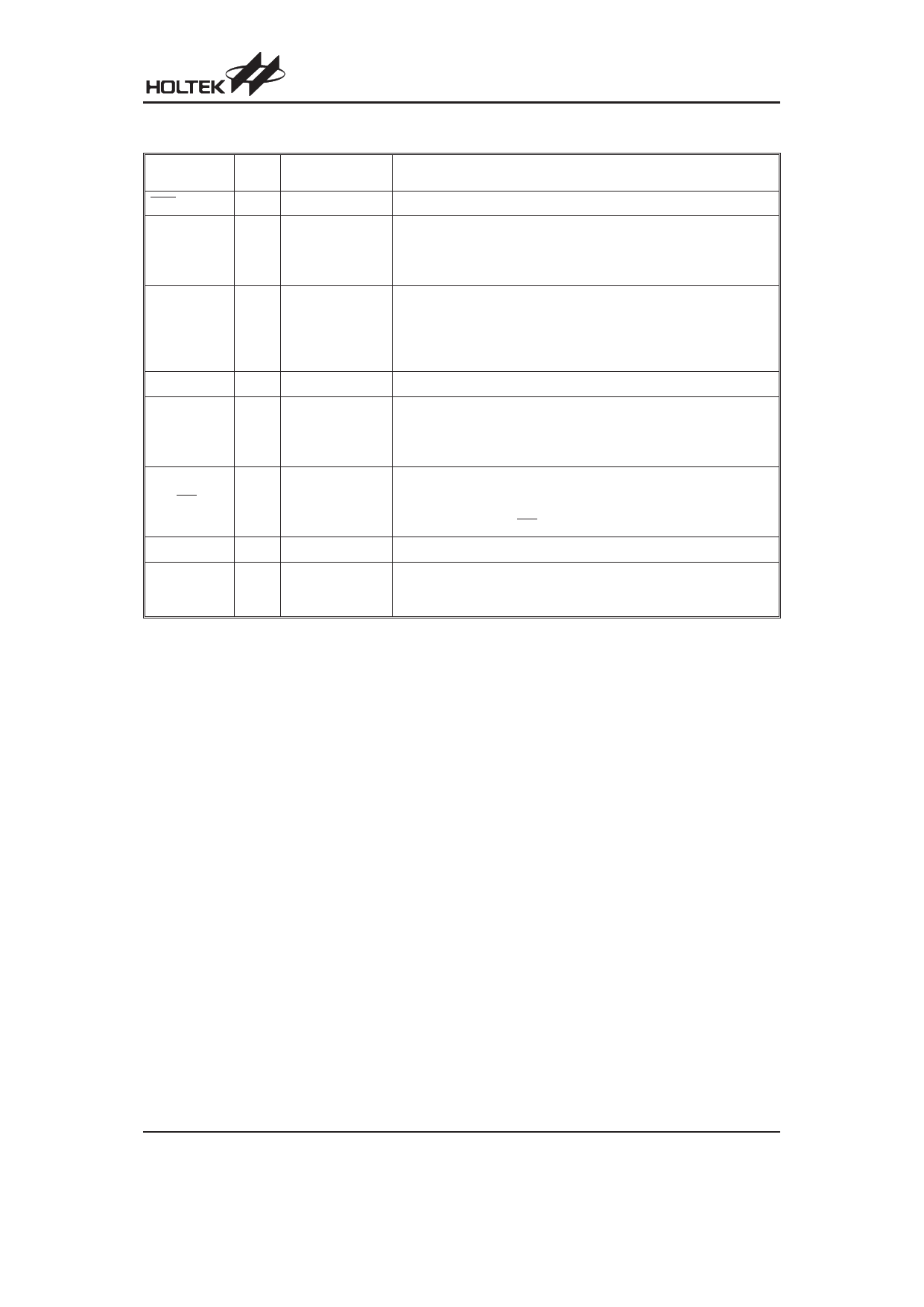
D.C. Characteristics
Symbol
Parameter
VDD
IDD
ISTB1
ISTB2
VIL1
VIH1
VIL2
VIH2
IOL
IOH1
IOH2
RPH
Operating Voltage
Operating Current
Standby Current (WDT Enabled)
Standby Current (WDT Disabled)
Input Low Voltage for I/O Ports
Input High Voltage for I/O Ports
Input Low Voltage (RES Ports)
Input High Voltage (RES Ports)
I/O Port Sink Current
I/O Port Source Current
I/O Port Source Current
Pull-high Resistance
Ta=25°C
Test Conditions
VDD
Conditions
Min.
¾
¾
2.2
3V No load, fSYS=4MHz
¾
3V No load, system HALT ¾
3V No load, system HALT ¾
¾
¾
0
¾
¾
0.8VDD
¾
¾
0
¾
¾
0.9VDD
3V VOL=0.1VDD
5
3V VOH=0.9VDD
-2
3V VOH=0.8VDD
-4
3V
¾
40
Typ.
¾
3
5
0.1
¾
¾
¾
¾
10
-5
-8
60
Max.
3.6
5
10
1
0.2VDD
VDD
0.4VDD
VDD
¾
¾
¾
80
Unit
V
mA
mA
mA
V
V
V
V
mA
mA
mA
kW
A.C. Characteristics
Symbol
Parameter
Test Conditions
VDD
Conditions
fSYS
System Clock
3V
¾
fTIMER Timer I/P Frequency (TMR0/TMR1) 3V 50% duty
tWDTOSC Watchdog Oscillator
3V
¾
tWDT1
Watchdog Time-out Period
(WDT OSC)
3V Without WDT prescaler
tWDT2 Watchdog Time-out Period (fSYS/4) 3V Without WDT prescaler
tRES
External Reset Low Pulse Width
¾
¾
tSST
System Start-up Timer Period
¾
Power-up, reset or
wake-up from HALT
tINT
Interrupt Pulse Width
¾
¾
tACC
Data ROM Access Time
¾
¾
Min.
400
0
45
11.5
¾
1
¾
1
1
Note: tSYS=1/(fSYS)
Typ.
¾
¾
90
23
1024
¾
1024
¾
¾
Ta=25°C
Max. Unit
4000 kHz
4000 kHz
180
ms
46
ms
¾
tSYS
¾
ms
¾
tSYS
¾
ms
¾
ms
Rev. 1.40
3
July 16, 2003
Share Link: 