PI5V330A データシートの表示(PDF) - Pericom Semiconductor
部品番号
コンポーネント説明
メーカー
PI5V330A Datasheet PDF : 7 Pages
| |||
PI5V330A
Low On-Resistance Wideband/Video
Quad 2-Channel Mux/DeMux
Maximum Ratings
(Above which the useful life may be impaired. For user guidelines, not tested.)
Storage Temperature ..........................................................–65°C to +150°C
Ambient Temperature with Power Applied .........................–40°C to +85°C
Supply Voltage to Ground Potential (Inputs & VCC Only)...–0.5V to +7.0V
Supply Voltage to Ground Potential (Outputs & D/O Only) –0.5V to +7.0V
DC Input Voltage ..................................................................–0.5V to +7.0V
DC Output Current.............................................................................120mA
Power Dissipation .................................................................................0.5W
Note:
Stresses greater than those listed under MAXIMUM RAT-
INGS may cause permanent damage to the device. This is
a stress rating only and functional operation of the device
at these or any other conditions above those indicated in the
operational sections of this specification is not implied. Ex-
posure to absolute maximum rating conditions for extended
periods may affect reliability.
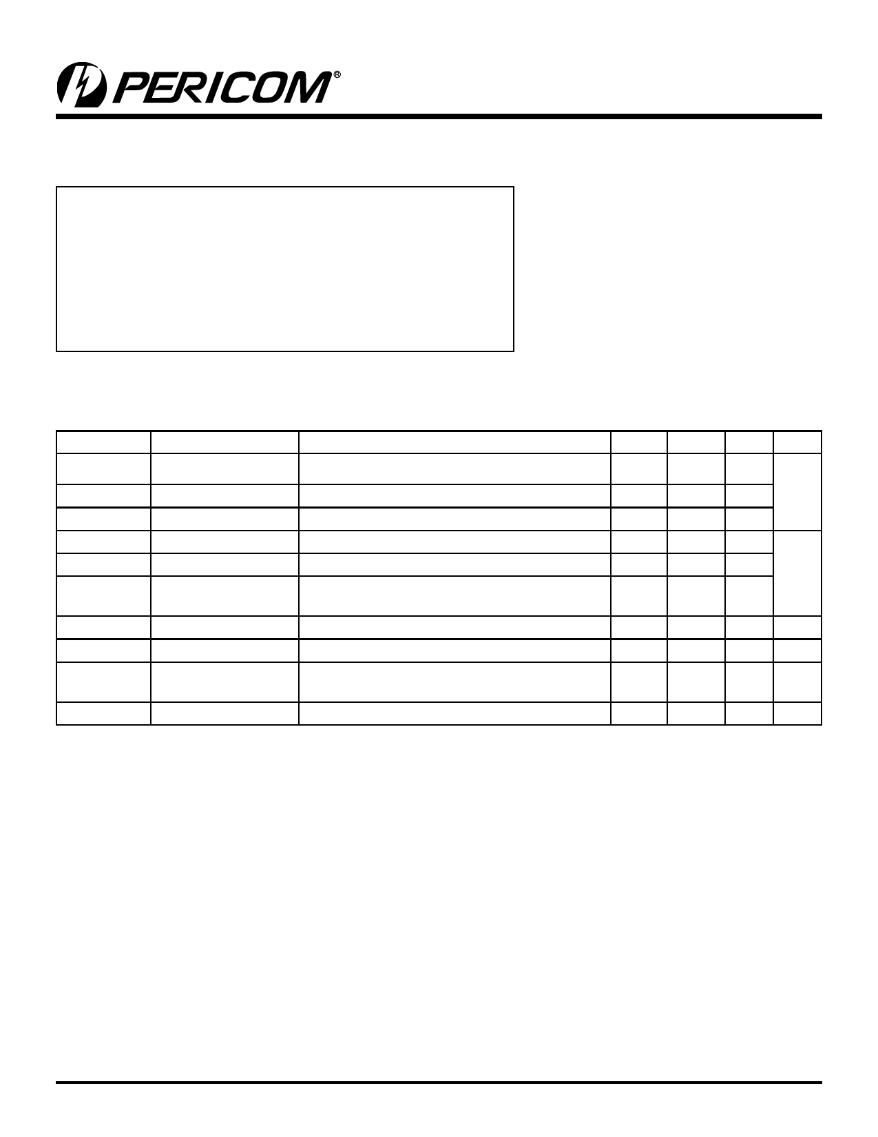
DC Electrical Characteristics (Over the Operating Range, TA = –40°C to +85°C, VCC = 5V ±5%)
Parameters
Description
Test Conditions(1)
Min. Typ.(2) Max. Units
VANALOG Analog Signal Range
0
2.0
VIH
Input HIGH Voltage Guaranteed Logic HIGH level
2.0
V
VIL
Input LOW Voltage Guaranteed Logic LOW Level
-0.5
0.8
IIH
Input HIGH Current VCC = Max., VIN = VCC
±1
IIL
Input LOW Current
VCC = Max., VIN = GND
IO
Analog Output
Leakage Currnet
0 ≤ S1, S2, or D ≤ VCC, Switch OFF
±1 µA
±1
VIK
Clamp Diode Voltage VCC = Min., IIN = -18mA
IOS
Short Circuit Current(3)
-0.7 -1.2
V
150
mA
VH
Input Hysteresis at
Control Pins
VCC = MIN., VIN = 1.0V RL = 75Ω, ION = 13 mA
3
7 mV
RON
Switch On-Resistance VCC = MIN., VIN = 2.0V RL = 75Ω, ION = 26 mA
3
7
10 Ω
Notes:
1. For Max. or Min. conditions, use appropriate value specified under Electrical Characteristics for the applicable device type.
2. Typical values are at VCC = 5.0V, TA = 25°C ambient and maximum loading.
3. Not more than one output should be shorted at one time. Duration of the test should not exceed one second.
4. Measured by the voltage drop between S1, S2, and D I/O pins at indicated current through the switch. On-Resistance is determined by the
lower of the voltages on the S1, S2, and D I/O pins.
2
PS8695B
03/01/05
Share Link: 