PLUS405-55A гғҮгғјгӮҝгӮ·гғјгғҲгҒ®иЎЁзӨәпјҲPDFпјү - Philips Electronics
йғЁе“Ғз•ӘеҸ·
гӮігғігғқгғјгғҚгғігғҲиӘ¬жҳҺ
гғЎгғјгӮ«гғј
PLUS405-55A Datasheet PDF : 16 Pages
| |||
Philips Semiconductors Programmable Logic Devices
Programmable logic sequencer
(16 Г— 64 Г— 8)
Product specification
PLUS405-55
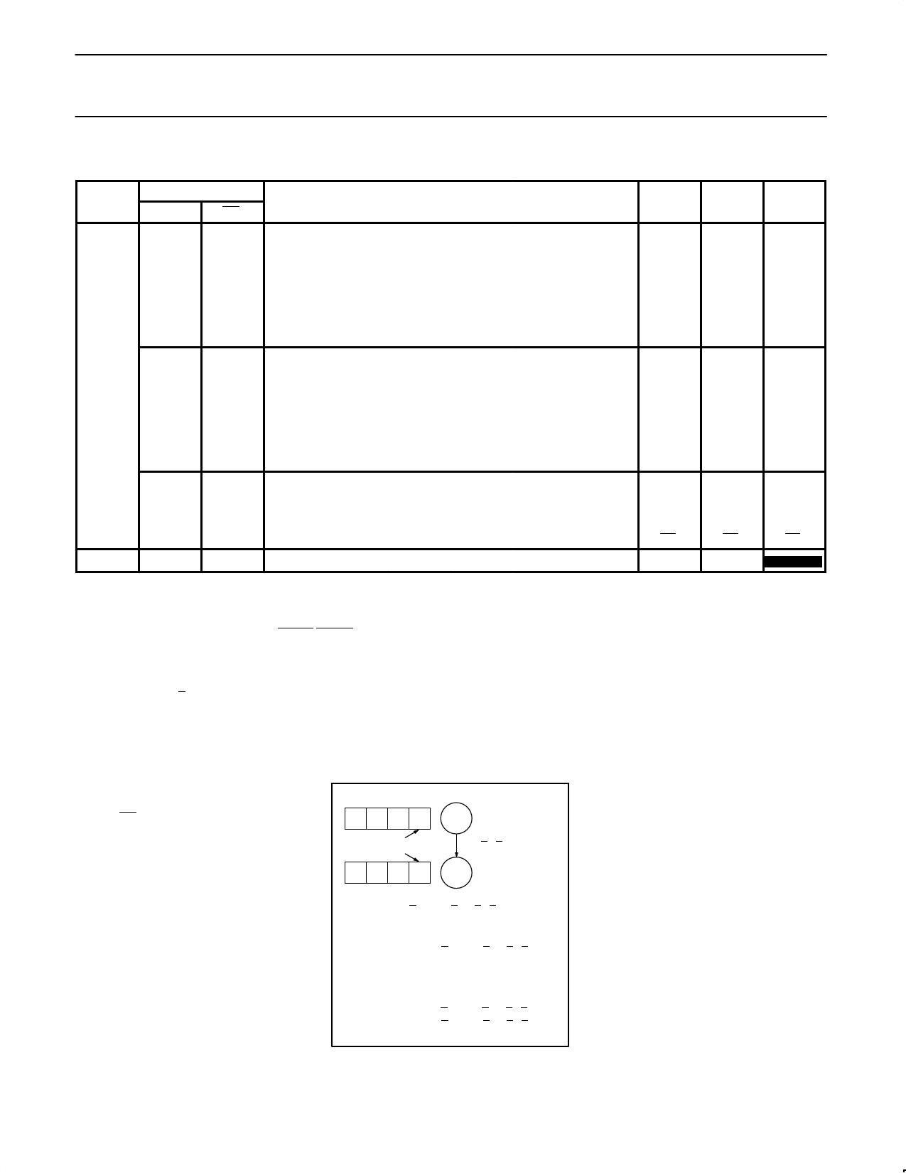
TRUTH TABLE 1, 2, 3, 4, 5, 6, 7
OPTION
VCC
INIT
OE
I10
I11
I12
CK
J
H
*
*
*
X
X
L
+10V
X
X
вҶ‘
X
L
+10V
X
X
вҶ‘
X
L
X
+10V
X
вҶ‘
X
L
X
+10V
X
вҶ‘
X
L
X
X
+10V
X
X
L
X
X
X
X
X
H
X
X
*
X
X
+5V
X
+10V
X
X
вҶ‘
X
X
+10V
X
X
вҶ‘
X
X
X
+10V
X
вҶ‘
X
X
X
+10V
X
вҶ‘
X
L
X
X
+10V
X
X
L
X
X
X
X
X
L
X
X
X
вҶ‘
L
L
X
X
X
вҶ‘
L
L
X
X
X
вҶ‘
H
L
X
X
X
вҶ‘
H
вҶ‘
X
X
X
X
X
X
X
K
QP
QF
F
X
H/L
H/L
QF
X
QP
L
L
X
QP
H
H
X
L
QF
L
X
H
QF
H
X
QP
QF
QP
X
QP
QF
QF
X
QP
QF
Hi-Z
X
QP
L
L
X
QP
H
H
X
L
QF
L
X
H
QF
H
X
QP
QF
QP
X
QP
QF
QF
L
QP
QF
QF
H
L
L
L
L
H
H
H
H
QP
QF
QF
X
H
H
NOTES:
1. Positive Logic:
S/R (or J/K) = T0 + T1 + T2 + . . . T63
Tn = (C0, C1) (I0, I1, I2, . . .) (P0, P1, . . . P7)
2. Either Initialization (Active-High) or Output Enable (Active-Low) are available, but not both. The desired function is a user-programmable
option.
3. вҶ‘ denotes transition from Low-to-High level.
4. * = H or L or +10V
5. X = DonвҖҷt Care (<5.5V)
6. H/L implies that either a High or a Low can occur, depending upon user-programmed selection (each State and Output Register individually
programmable).
7. When using the Fn pins as inputs to the State and Output Registers in diagnostic mode, the F buffers are 3-Stated and the indicated levels
on the output pins are forced by the user.
VIRGIN STATE
A factory-shipped virgin device contains all
fusible links intact, such that:
1. INIT/OE is set to INIT. In order to use the
INIT function, the user must select either
the PRESET or the RESET option for
each flip-flop. Note that regardless of the
user-programmed initialization, or even if
the INIT function is not used, all registers
are preset to вҖң1вҖқ by the power-up
procedure.
2. All transition terms are inactive (0).
3. All S/R (or J/K) flip-flop inputs are
disabled (0).
4. The device can be clocked via a Test
Array preprogrammed with a standard
test pattern.
5. Clock 2 is inactive.
LOGIC FUNCTION
Q3 Q2 Q1 Q0
1010
STATE REGISTER
SR PRESENT STATE
AвӢ…BвӢ…CвӢ…...
0001
Sn + 1 NEXT STATE
SET Q0: J0 = (Q2 вӢ… Q1 вӢ… Q0) вӢ… A вӢ… B вӢ… C . . .
K0 = 0
RESET
Q1: J1
K1
=
=
0
(Q3
вӢ…
Q2
вӢ…
Q1
вӢ…
Q0)
вӢ…
A
вӢ…
B
вӢ…
C
.
.
.
HOLD Q2: J2 = 0
K2 = 0
RESET
Q3:
J3
K3
=
=
(Q3
(Q3
вӢ…
вӢ…
Q2
Q2
вӢ…
вӢ…
Q1
Q1
вӢ…
вӢ…
Q0)
Q0)
вӢ…
вӢ…
A
A
вӢ…
вӢ…
B
B
вӢ…
вӢ…
C
C
.
.
.
.
.
.
October 22, 1993
182
Share Link: 