PS320CSA データシートの表示(PDF) - Pericom Semiconductor
部品番号
コンポーネント説明
メーカー
PS320CSA Datasheet PDF : 6 Pages
| |||
PS320/PS321/PS322
12345678901234567890123456789012123456789012345678901234567890121234567890123456789012P34r56e7c8i9s0i1o21n23,4D56u78a90l1-2S3u45p67p89ly012A34n56a7l8o90g12S12w34i5t6c7h89e01s2
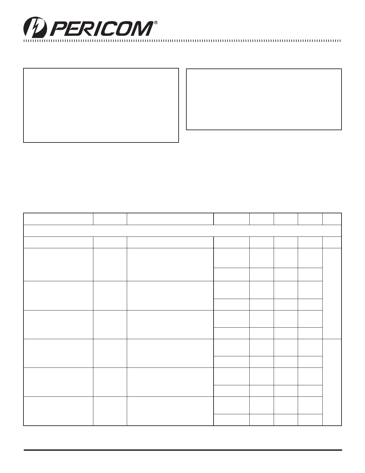
Absolute Maximum Ratings
Voltages Referenced to V
V+ ...................................................................... -0.3V to +17V
VIN, VCOM, VNC, VNO(1) ............................. (V-) -2V to (V+) +2V
............................................... or 30mA, whichever occurs first
Current (any terminal) ..................................................... 30mA
Peak Current, COM, NO, NC
(pulsed at 1ms, 10% duty cycle) ................................... 100mA
ESD per Method 3015.7 ............................................. > 2000V
Thermal Information
Continuous Power Dissipation
Plastic DIP (derate 6mW/ ºC above +70ºC) .................... 500mW
Narrow SO (derate 6mW/ ºC above +70ºC) .................... 450mW
MSOP (derate 4mW/ ºC above +70ºC) ........................... 330mW
Storage Temperature ........................................ -65ºC to +150ºC
Lead Temperature (soldering, 10s) ................................ +300ºC
Note 1:
Signals on NC, NO, COM, or IN exceeding V+ or V- are clamped
by internal diodes. Limit forward diode current to maximum current
rating
Caution:
Stresses beyond those listed under Absolute Maximum Ratings may cause permanent damage to the device. This is a stress only rating and operation
of the device at these or any other conditions beyond those indicated in the operational sections of this specification is not implied.
Electrical Specifications - Dual Supplies (V± = ± 5V ±10%, VINH = 3.5V, VINL = 1V)
Parameter
Symbol
Conditions
Temp. (°C) Min.(2) Typ.(1) Max.(2) Units
Analog Switch
Analog Signal Range (3)
VAN ALO G
ON-Resistance
RO N
V+ = 4.5V, V = 4.5V,
VNO or VNC = ±3.5V
ICOM = 1mA,
Full
V
V+
V
25
16
35
Full
45
ON-Resistance Match
Between Channels(4)
DRON
V+ = 5V, V = 5V
VNO or VNC = ±3V,
ICOM = 1mA,
25
Full
0.3
2 ohm
4
V+ = 5V, V = 5V,
25
ON-Resistance Flatness(5) RFLAT(ON)
ICOM = 1mA ,
VNO or VNC = ±3V
Full
1
4
6
NO or NC Off Leakage INO(OFF) or
Current(6)
IN C (O FF)
V+ = 5.5V, V = 5.5V,
VCOM = ±4.5V,
VNO or VNC = ±4.5V
25
0.1 0.01 0.1
Full
5
5
COM Off Leakage
Current(6)
IC O M(O FF)
V+ = 5.5V, V = 5.5V
VCOM = ±4.5V,
VNO or VNC = ±4.5V
25
0.1 0.01 0.1 nA
Full
5
5
COM On Leakage
Current(6)
IC O M(O N )
V+ = 5.5V , V = 5.5V,
VCOM = ±4.5V
VNO or VNC = ±4.5V
25
0.2 0.04 0.2
Full
10
10
continued next page
2
PS8183E 06/10/02
Share Link: 