MF0015M-03AT データシートの表示(PDF) - MITSUBISHI ELECTRIC
部品番号
コンポーネント説明
メーカー
MF0015M-03AT Datasheet PDF : 29 Pages
| |||
MITSUBISHI STORAGE CARD
ATA Register Specifications
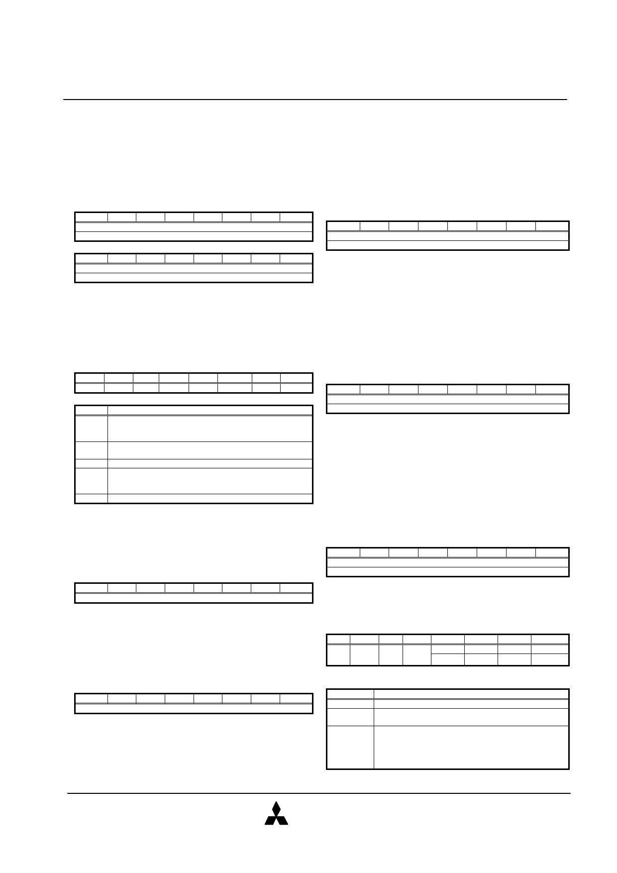
Data Register
This register is a 16 bit register which is used to transfer
data blocks between the card data buffer and the host.
Data may be transferred by either a series of word
accesses to the Data register or a series of byte accesses
to the Data register.
D15 D14 D13 D12 D11 D10 D9
D8
Data Word
Odd Data Byte
D7
D6
D5
D4
D3
D2
D1
D0
Data Word
Data Byte
Error Register
This register contains additional information about the
source of an error which has occurred in processing of the
preceding command. This register should be checked by
the host when ERR bit in the Status register is set. The
Error register is a read only register.
D7
D6 D5 D4
D3
BBK UNC 0 IDNF
0
D2
ABRT
D1
D0
0 AMNF
Field
BBK
UNC
IDNF
ABRT
AMNF
function
This bit is set when a Bad Block is detected in requested ID
field. Host can not read/write on data area that is marked as
a Bad Block.
This bit is set when Uncorrectable error is occurred at
reading the card.
The requested sector ID is in error or cannot be found.
This bit is set if the command has been aborted because of
the card status condition. (Not ready, Write fault, etc.) or
when an invalid command has been issued.
This bit is set in case of a general error.
Feature Register
This register is written by the host to provide command
specific information to the drive regarding features of the
drive which the host wish to utilize. The Feature register is
a write only register.
D7
D6
D5
D4
D3
D2
D1
D0
Feature byte
Sector Count Register
This register is written by the host with the number of
sectors or blocks to be processed in the subsequent
command. After the command is complete, the host may
read this register to obtain the count of sectors left
unprocessed by the command.
D7
D6
D5
D4
D3
D2
D1
D0
Sector Count
ATA PC CARDS
Sector Number Register
This register is written by the host with the starting sector
number to be used in the subsequent Cylinder-Head-
Sector command. After the command is complete, the
host may read the final sector number from this register.
When logical block addressing is used, this register is
written by the host with bit7 to 0 of the starting logical
block number and contains bit7 to 0 of the final logical
block number after the command is complete.
D7
D6
D5
D4
D3
D2
D1
D0
Sector Number
Logical Block Number bits A07-A00(LBA Addressing)
Cylinder Low Register
This register is written by the host with the low-order byte
of the starting cylinder address to be used in the
subsequent Cylinder-Head-Sector command. After the
command is complete, the host may read the low-order
byte of the final cylinder number from this register. When
logical block addressing is used, this register is written by
the host with bits15 to 8 of the starting logical block
number and contains bits15 to 8 of the final logical block
number after the command complete.
D7
D6
D5
D4
D3
D2
D1
D0
Cylinder Low Byte
Logical Block Number bits A15-A08(LBA Addressing)
Cylinder High Register
This register is written by the host with the high-order byte
of the starting cylinder address to be used in the
subsequent Cylinder-Head-Sector command. After the
command is complete, the host may read the high-order
byte of the final cylinder number from this register. When
logical block addressing is used, this register is written by
the host with bits 23 to 16 of the starting logical block
number and contains bits23 to 16 of the final logical block
number after the command is complete.
D7
D6
D5
D4
D3
D2
D1
D0
Cylinder High Byte
Logical Block Number bits A23-A16(LBA Addressing)
Drive/Head Register
The Drive/Head register is used to specify the selected
drive of a pair of drives sharing a set of registers.
D7 D6 D5 D4
D3
D2
D1
D0
X LBA X DRV HS3
HS2
HS1
HS0
LBA27 LBA26 LBA25 LBA24
Field
X
LBA
DRV
function
Undefined . “0” or “1”.
This bit is “0” for CHS addressing and “1” for Logical
Block addressing.
This bit is number of the drive which the host has
selected. When DRV is cleared, Drive0 is selected.
When DRV is set, Drive1 is selected. The card is
selected to be Drive0 or to be Drive1 using the “Copy”
field of the PC Card Socket Copy Register.
MITSUBISHI
ELECTRIC
15
1997.Nov. Rev. 1.2
Share Link: 