NJG1704KC1-L1 データシートの表示(PDF) - Japan Radio Corporation
部品番号
コンポーネント説明
メーカー
NJG1704KC1-L1 Datasheet PDF : 17 Pages
| |||
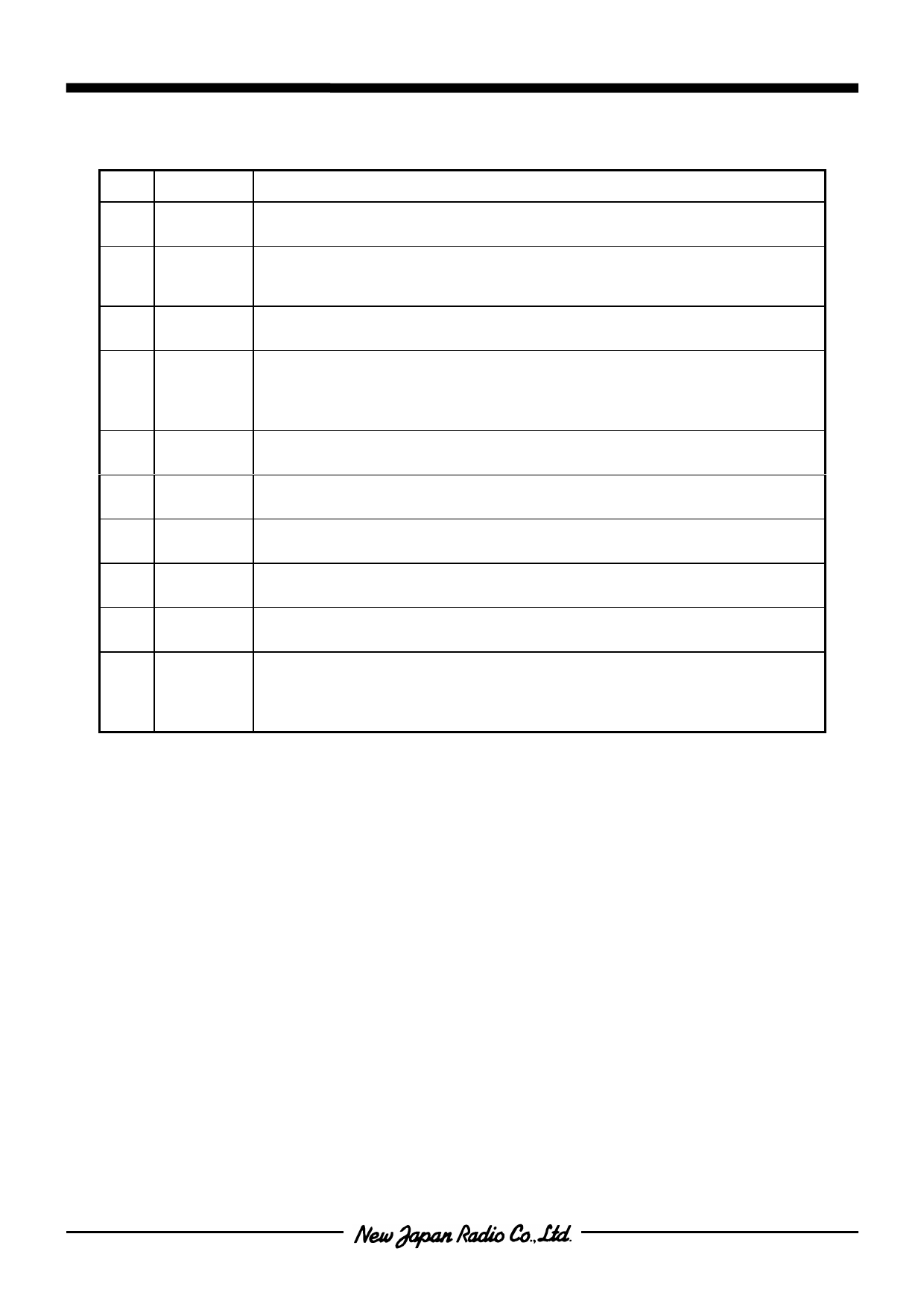
nTERMINAL INFORMATION
NJG1704KC1
No. SYMBOL
FUNCTION
1
LNAIN RF input terminal of LNA. An external matching circuit is required.
Terminal for the bypass capacitor of LNA. The bypass capacitor C1 as
2 LNACAP shown in test circuits, should be connected to this terminal as close as
possible.
3
GND Ground terminal(0V)
IF signal output terminal. The IF signal is output through external matching
4
IFOUT
circuit connected to this terminal. Please connect inductances L7, L8 and
power supply as shown in test circuits, since this terminal is also the
terminal of mixer power supply.
5
VLO
Power supply terminal for local amplifier. Please place R1 and L10 as
shown in test circuits at very close to this terminal.
6
LOIN
Local signal input terminal to local amplifier. An external matching circuit is
required.
7
GND Ground terminal(0V)
8
MIXIN RF signal input terminal to mixer. An external matching circuit is required.
9
GND Ground terminal(0V)
Signal output terminal of LNA. The RF signal from LNA is output through
10
LNAOUT
external matching circuit connected to this terminal. Please connect
inductances L3, L4 and power supply as shown in test circuits, since this
terminal is also the terminal of LNA power supply.
CAUTION
1) Ground terminal (No.3, 7, 9) should be connected to the ground plane as low
inductance as possible.
-3-
Share Link: 