UPB1511TB-E3(2002) データシートの表示(PDF) - NEC => Renesas Technology
部品番号
コンポーネント説明
メーカー
UPB1511TB-E3
(Rev.:2002)
(Rev.:2002)
NEC => Renesas Technology

UPB1511TB-E3 Datasheet PDF : 3 Pages
| |||
UPB1511TB
ABSOLUTE MAXIMUM RATINGS1
SYMBOLS
PARAMETERS
UNITS RATINGS
VCC
Supply Voltage
TA = +25° C
V
3.6
VIN
Input Voltage
TA = +25° C, SW Pin
V
3.6
PD
Total Power Dissipation2
mW
200
(TA = +85° C)
TA
Operating Ambient Temp. °C -40 to +85
TSTG
Storage Temperature
°C -55 to +150
Notes:
1. Operation in excess of any one of these conditions may result in
permanent damage.
2. Mounted on double sided copper clad 50 x 50 x 1.6mm epoxy
glass PWB
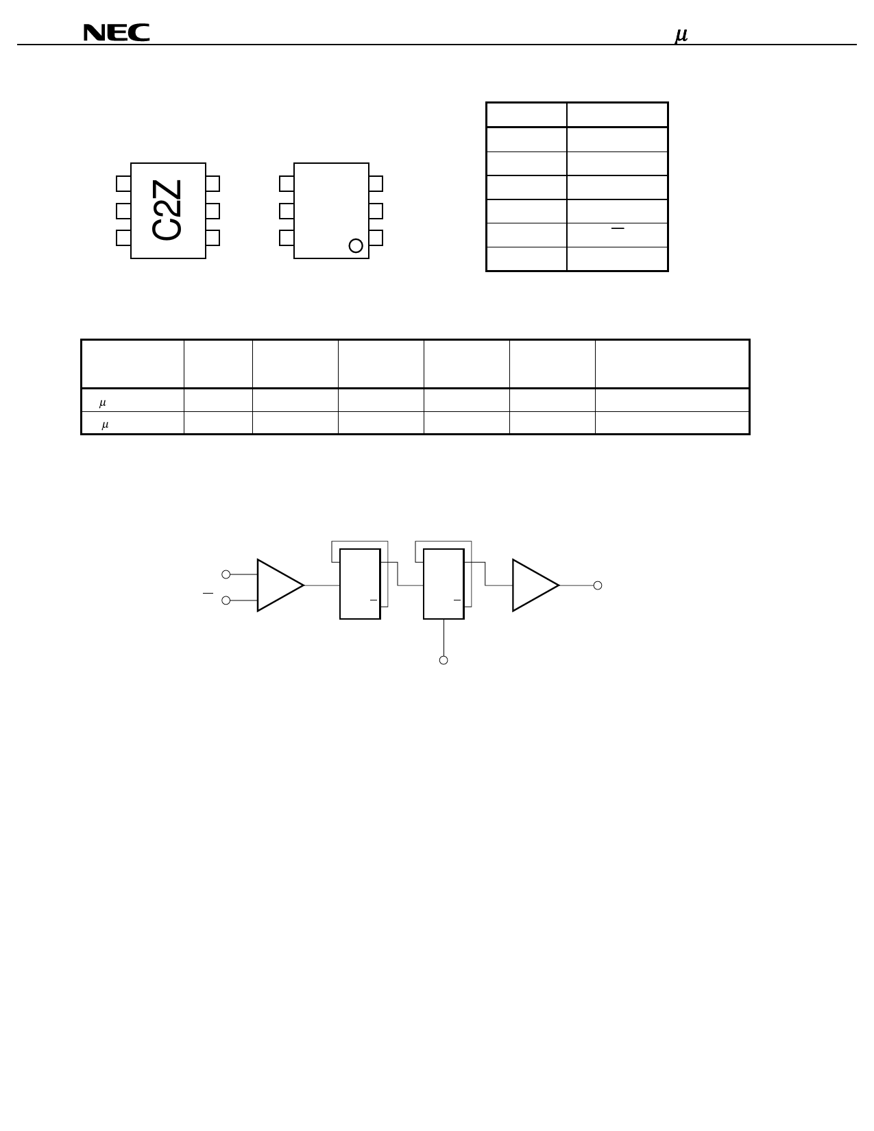
INTERNAL BLOCK DIAGRAM
DQ
DQ
IN
CLK
CLK
IN
Q
Q
OUT
RECOMMENDED
OPERATING CONDITIONS
SYMBOLS PARAMETERS
UNITS MIN TYP MAX
VCC Supply Voltage
V 2.4 3.0 3.3
TA
Operating Ambient Temp. °C -40 +25 +85
SYSTEM APPLICATION EXAMPLE
LNA
RX
SW
TX
PA
VCO
DEMOD.
I
Q
÷N PLL
VCO
PLL
÷N UPB1511TB
I
0˚
Phase
Shifter
90˚
Q
SW
PRODUCT LINE-UP
PART NUMBER
ICC
(mA)
UPB1509 GV
5.0
UPB1511 TB
3.5
VCC
(V)
2.2 to 5.5
2.4 to 3.3
÷2
fIN
(MHZ)
50 to 700
50 to 700
÷4
fIN
(MHZ)
50 to 800
50 to 800
÷8
fIN
(MHZ)
50 to 1000
-
PACKAGE
8-pin SSOP
6-pin super minimold
PIN EXPLANATIONS
PIN NO.
1
SYMBOL
OUT
APPLIED
VOLTAGE (V)
–
2
GND
0
3
SW
H/L
4
IN
–
5
IN
–
6
VCC
2.4 TO 3.3
FUNCTIONS AND EXPLANATION
Divided Frequency Output Pin. This pin is designed as an emitter follower output
and can deliver 0.2 VP-P minimum into a 200 Ω load.
This pin should be coupled to the load device with a capacitor (example: 1000 pF)
for DC cut.
Ground Pin. Ground pattern on the board should be as wide as possible to
minimize ground impedance.
Divide Ratio Control Pin. Divide ratio can be determined by the following applied
level to these pins.
Divide ratio
SW
H
L
1/2 1/4
These pins must be each equipped with bypass capacitor to minimize
their impedance.
Signal Input Pin. This pin should be coupled to the signal source with a capacitor
(example: 1000 pF) for DC cut.
Signal Input Bypass Pin. This pin must be equipped with a bypass capacitor
(example: 1000 pF) to minimize ground impedance.
Power Supply Pin. This pin must be equipped with a bypass capacitor
(example: 1000 pF) to minimize ground impedance.
Share Link: