REF02 データシートの表示(PDF) - Analog Devices
部品番号
コンポーネント説明
メーカー
REF02 Datasheet PDF : 16 Pages
| |||
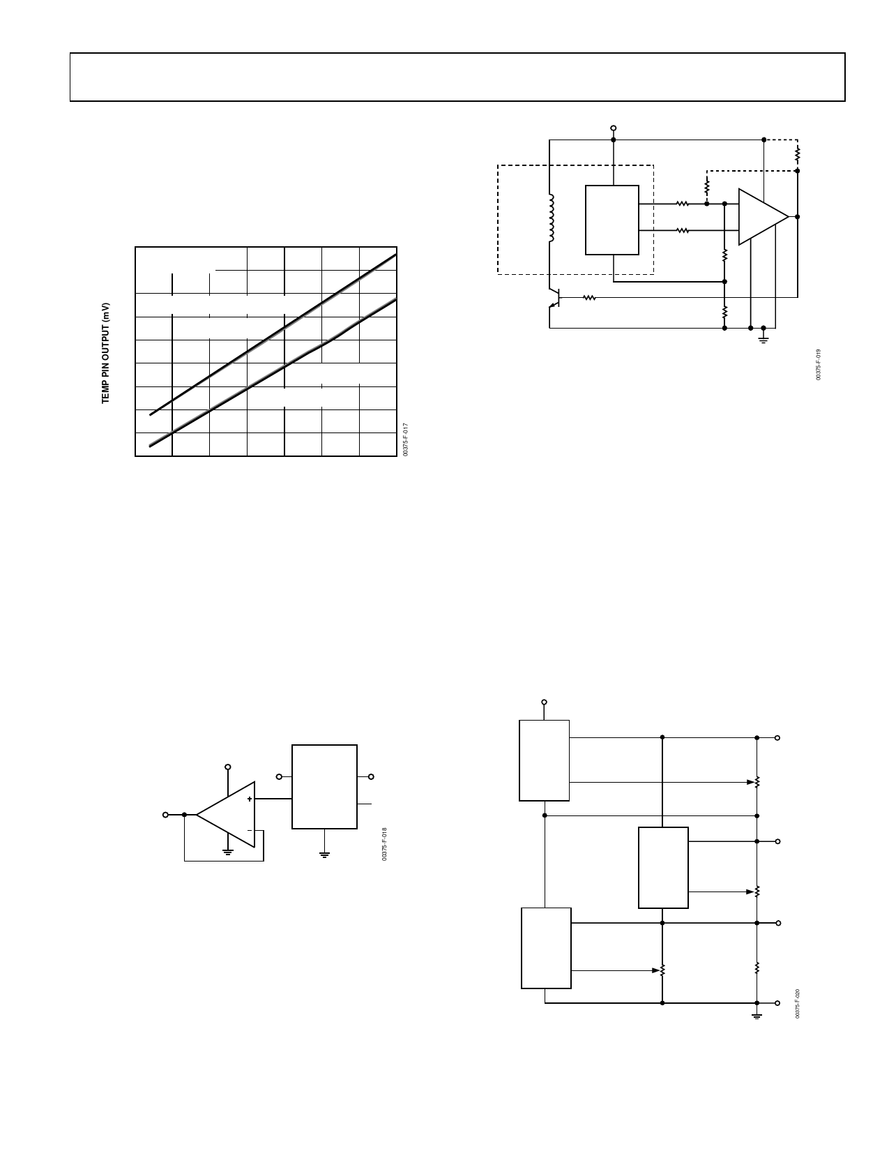
TEMPERATURE MONITORING
The REF02 provides a TEMP output (Pin 3) that varies linearly
with temperature. This output can be used to monitor the
temperature change in the system. The voltage at VTEMP is
approximately 550 mV at 25°C, and the temperature coefficient
is approximately 1.96 mV/°C (see Figure 18).
850
VIN = 9V
800 SAMPLE SIZE = 6
750
Z PACKAGE AND 833 PRODUCT
700
∆VTEMP/∆T = 2.1mV/°C
650
600
∆VTEMP/∆T = 1.96mV/°C
550
J, S, AND P PACKAGES
500
450
400
–50 –25
0
25
50
75
100
125
TEMPERATURE (°C)
Figure 18. Voltage at TEMP Pin vs. Temperature
A voltage change of 39.2 mV at the TEMP pin corresponds to a
20°C change in temperature.
The TEMP function is provided as a convenience rather than a
precise feature. Since the voltage at the TEMP node is acquired
from the band gap core, current pulling from this pin has a
significant effect on VOUT. Care must be taken to buffer the
TEMP output with a suitable low bias current op amp, such as
the AD8601, AD820, or OP1177. Using any of these three op
amps results in less than a 100 µV change in ΔVOUT (see
Figure 19). Without buffering, even tens of microamps drawn
from the TEMP pin can cause VOUT to fall out of specification.
U1
15V
REF02
VIN
VIN
VOUT
VO
VTEMP
1.9mV/°C
V+
OP1177
U2
V–
TEMP TRIM
GND
Figure 19. Temperature Monitoring
REF02
V+ (12V TO 32V)
HEATING
ELEMENT
2
VIN VO 6
REF02
TEMP 3
GND
(SEE NOTE 1) 4
R7
27kΩ
R1
(9.2kΩ)
R6
R3
(1.3kΩ)
R2
1.5kΩ
2
3
+
8
V+
CMP02V–
–
4
7
1
R5
2.2kΩ
R4
2.7kΩ
NOTES
1. REF02 SHOULD BE THERMALLY CONNECTED
TO SUBSTANCE BEING HEATED.
2. NUMBERS IN PARENTHESES ARE FOR A
SETPOINT TEMPERATURE OF 60°C.
3. R3 = R1 || R2 || R6
Figure 20. Temperature Controller
REFERENCE STACK WITH EXCELLENT LINE
REGULATION
Two REF01s and one REF02 can be stacked to yield 5.00 V,
15.00 V, and 25.00 V outputs. An additional advantage is near-
perfect line regulation of the 5.0 V and 15.0 V output. A 27 V to
55 V input change produces an output change that is less than
the noise voltage of the devices. A load bypass resistor (RB)
provides a path for the supply current (ISY) of the 15.00 V
regulator.
In general, any number of REF01s and REF02s can be stacked
this way. For example, 10 devices yield 10 outputs in 5 V or 10 V
steps. The line voltage can change from 100 V to 130 V. Care
must be taken, however, to ensure that the total load currents
do not exceed the maximum usable current (typically 21 mA).
27V TO 55V
2
VIN
6
VO
REF02
5
TRIM
GND
4
2
VIN VO 6
15V
10kΩ
10V
2
VIN
6
VO
REF02
5
TRIM
GND
4
REF02
5
TRIM
GND
4
10kΩ
10kΩ
5V
RB
6.8kΩ
Figure 21. Reference Stack
Rev. I | Page 11 of 16
Share Link: 