RF2196PCBA-41X データシートの表示(PDF) - RF Micro Devices
部品番号
コンポーネント説明
メーカー
RF2196PCBA-41X Datasheet PDF : 12 Pages
| |||
RF2196
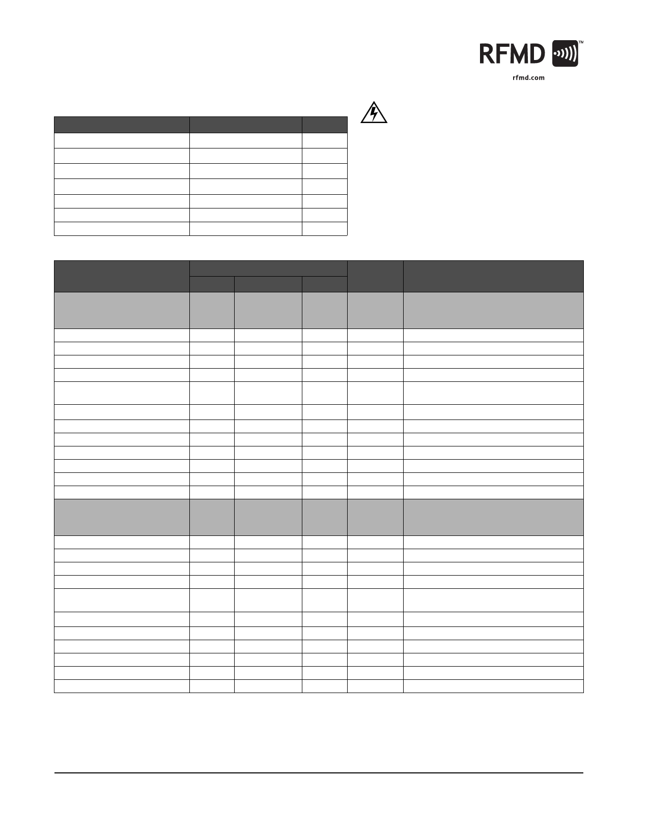
Absolute Maximum Ratings
Parameter
Supply Voltage (RF off)
Supply Voltage (POUT≤31dBm)
Mode Voltage (VMODE)
Control Voltage (VREG)
Input RF Power
Operating Case Temperature
Storage Temperature
Rating
+8.0
+5.2
+4.2
+3.0
+10
-30 to +110
-30 to +150
Unit
VDC
VDC
VDC
VDC
dBm
°C
°C
Caution! ESD sensitive device.
Exceeding any one or a combination of the Absolute Maximum Rating conditions may
cause permanent damage to the device. Extended application of Absolute Maximum
Rating conditions to the device may reduce device reliability. Specified typical perfor-
mance or functional operation of the device under Absolute Maximum Rating condi-
tions is not implied.
RoHS status based on EUDirective2002/95/EC (at time of this document revision).
The information in this publication is believed to be accurate and reliable. However, no
responsibility is assumed by RF Micro Devices, Inc. ("RFMD") for its use, nor for any
infringement of patents, or other rights of third parties, resulting from its use. No
license is granted by implication or otherwise under any patent or patent rights of
RFMD. RFMD reserves the right to change component circuitry, recommended appli-
cation circuitry and specifications at any time without prior notice.
Parameter
High Power State
(VMODE Low)
Frequency Range
Linear Gain
Second Harmonic
Third Harmonic
Maximum Linear Output Power
(CDMA Modulation)
Total Linear Efficiency
Adjacent Channel Power Rejection
Input VSWR
Output VSWR
Noise Power
Low Power State
(VMODE High)
Frequency Range
Linear Gain
Second Harmonic
Third Harmonic
Maximum Linear Output Power
(CDMA Modulation)
Max ICC
Adjacent Channel Power Rejection
Input VSWR
Output VSWR
Specification
Min.
Typ.
Max.
1850
25
29
27
-50
-63
35
-46
-62
<2:1
-141
1910
-44
-56
10:1
6:1
1850
16
16
20
-45
-60
20
160
< -50
< -60
2:1
1910
-46
-58
10:1
6:1
Unit
MHz
dB
dBc
dBc
dBm
%
dBc
dBc
Condition
Case T=25°C, VCC=3.4V, VREG=2.85V,
VMODE=0V to 0.5V, Freq=1850MHz to
1910MHz (unless otherwise specified)
POUT = 29 dBm
ACPR @ 1.25 MHz
ACPR @ 2.25 MHz
dBm/Hz
MHz
dB
dBc
dBc
dBm
No damage.
No oscillations. >-70dBc
At 80MHz offset.
Case T=25°C, VCC=3.4V, VREG=2.85V,
VMODE=2V to 3V, Freq=1850MHz to
1910MHz (unless otherwise specified)
mA
POUT=+16dBm (all currents included)
dBc
ACPR @ 1.25 MHz
dBc
ACPR @ 2.25 MHz
No damage.
No oscillations. >-70dBc
2 of 12
7628 Thorndike Road, Greensboro, NC 27409-9421 · For sales or technical
support, contact RFMD at (+1) 336-678-5570 or sales-support@rfmd.com.
Rev A3 DS070730
Share Link: 