RF212 データシートの表示(PDF) - Unspecified
部品番号
コンポーネント説明
メーカー
RF212 Datasheet PDF : 9 Pages
| |||
RF212
Image-Reject Front End
NC
1
20
VCC
GND
2
19
GND
GND
3
18
STEPSEL
LNA900IN
4
VCC
5
17
IFOUT+
16
IFOUT-
VCC
6
15
GND
GAINSEL
7
LNA1800IN
8
14
BANDSEL1
13
LOIN
GND
9
ENA 10
12
LOGND
11
NC
C067
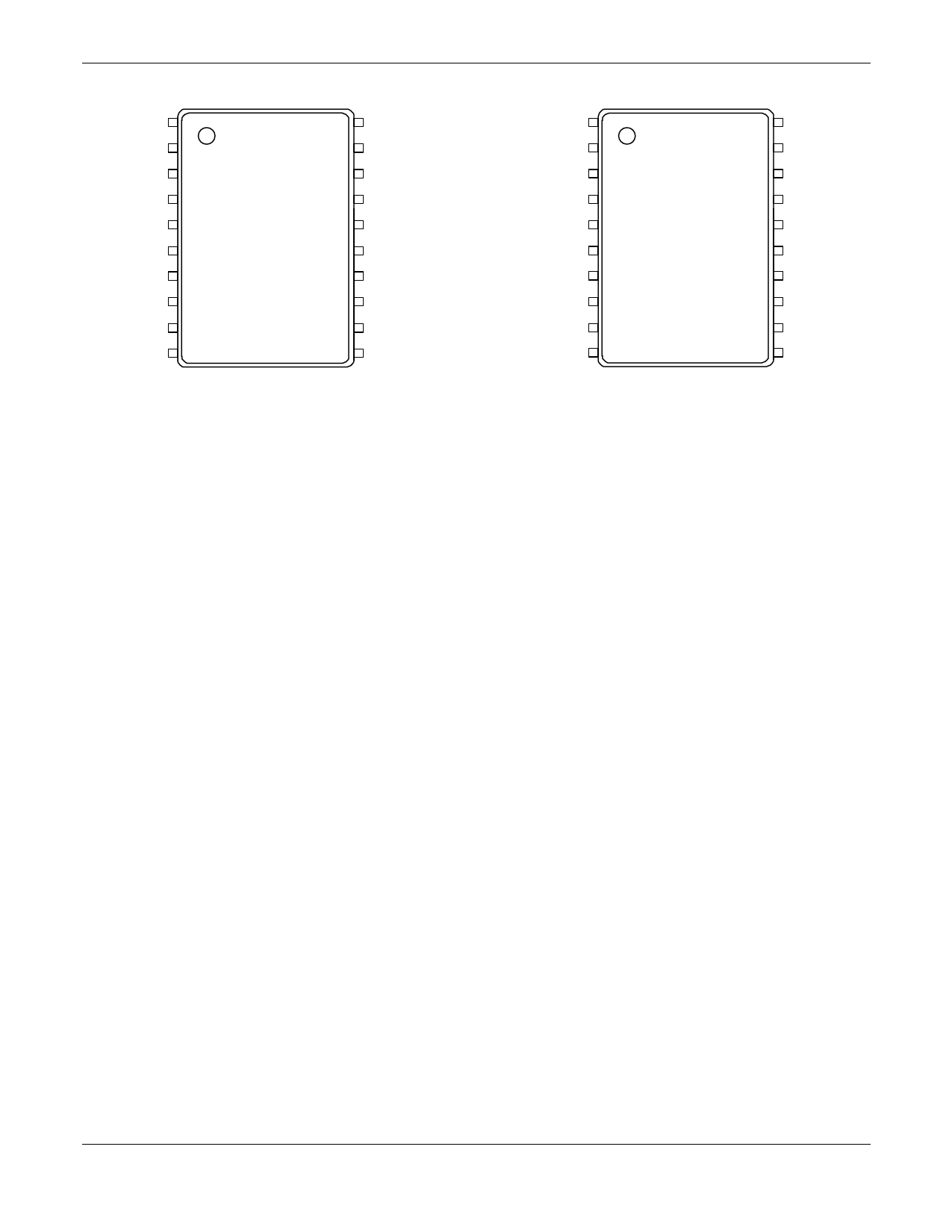
Figure 3. RF212 Dual-Band Device Pin Configuration − 20-Pin
ETSSOP
Technical Description
Both RF212 devices form front ends of a dual-band or a tri-band
super-heterodyne receiver. The RF212 dual-band device is
optimized for an EGSM900/DCS1800 design, while the RF212
tri-band device is suitable for EGSM900, DCS1800, and PCS
1900. Each frequency band has its own separate front-end
receiver path. Each receiver path contains an LNA, an image-
reject filter, and a mixer. The IF and LO ports are common to all
frequency bands. The image rejection achievable by this front-
end design without any additional external components is 35 dB
minimum for an IF of 400 MHz. Both devices operate over a
supply voltage range of 2.7 V to 3.6 V.
The RF212 dual-band device has one band selection pin
(BANDSEL1 on pin 14). When BANDSEL1 is set to logic “0,” the
EGSM900 receiver path is active. The LO frequency needs to
be higher than the RF input frequency (i.e., a high side injection
is used). When BANDSEL1 is set to logic “1,” the DCS1800
receiver path is active. The LO frequency needs to be less than
the RF input frequency (i.e., a low-side injection is used). With a
400 MHz IF, this arrangement allows a single, wide-range
Voltage Controlled Oscillator (VCO) to be used for each band of
operation.
NC 1
20
VCC
GND
2
19 GND
GND
3
18
STEPSEL
LNA900IN
4
17
IFOUT+
VCC 5
16
IFOUT-
VCC
6
15
BANDSEL2
GAINSEL
7
14
BANDSEL1
LNA1800IN
8
13
LOIN
LNA1900IN
9
12
LOGND
ENA 10
11 NC
C122
Figure 4. RF212 Tri-Band Device Pin Configuration – 20-Pin
ETSSOP
Similarly, the RF212 tri-band device has two band selection pins
(BANDSEL1 and BANDSEL2, pins 14 and 15, respectively). The
EGSM900 path uses the high side injection for the LO, while
DCS1800 and PCS1900 paths use the low side injection. Tables
1 and 2 provide the frequency band selection settings for the
dual and tri-band devices, respectively.
All the LNAs have switchable gain. The gain mode is selectable
using the GAINSEL signal (pin 7). Low gain mode is selected by
driving the GAINSEL signal to a logic “1”; high gain mode is
selected by driving the signal to a logic “0.” Depending on the
need of the handset design on the gain distribution, the gain
step between the high gain and low gain modes can be set to
either a 12 dB step or a 20 dB step. This gain step is selectable
with the STEPSEL signal (pin 18).
Electrical and Mechanical Specifications ________________
The RF212 signal pin assignments and functional pin
descriptions are found in Table 3 (dual-band) and Table 4 (tri-
band). The absolute maximum ratings of the RF212 are
provided in Table 5, the operating conditions are specified in
Table 6, and electrical specifications are provided in Table 7.
Figure 3 shows the diagram for a typical application circuit using
the RF212 front end. Figure 4 provides the package dimensions
for both of the 20-pin ETSSOP devices.
ESD Sensitivity
The RF212 is a static-sensitive electronic device. Do not operate
or store near strong electrostatic fields. Take proper ESD
precautions.
2
May 24, 2000
Conexant
Proprietary Information and Specifications are Subject to Change
100780D
Share Link: 