RF2377(Rev_A9) データシートの表示(PDF) - RF Micro Devices
部品番号
コンポーネント説明
メーカー
RF2377 Datasheet PDF : 8 Pages
| |||
RF2377
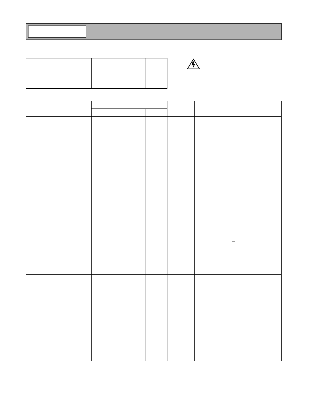
Absolute Maximum Ratings
Parameter
Supply Voltage
DC Current
Operating Ambient Temperature
Storage Temperature
Rating
0 to +5.0
100
-20 to +85
-40 to +150
Unit
VDC
mA
°C
°C
Caution! ESD sensitive device.
RF Micro Devices believes the furnished information is correct and accurate
at the time of this printing. However, RF Micro Devices reserves the right to
make changes to its products without notice. RF Micro Devices does not
assume responsibility for the use of the described product(s).
Parameter
Specification
Unit
Min.
Typ.
Max.
Condition
Overall
4
Usable Frequency Range
Linear Gain Control Range
800 to 2200
50
Gain Control Slope
70
TDMA
Operating Frequency
1880
Maximum Small Signal Gain
22
24
27
Input VSWR
1.5:1
2.5:1
Output IP3
+23
+26
Noise Figure
7
Maximum Average Output Power
+8
Adjacent Channel Power
Rejection
-33
-32
Alternate Channel Power
Rejection
-61
-57
CDMA
Operating Frequency
1880
Maximum Small Signal Gain
22
24
27
Input VSWR
1.5:1
2.5:1
Output IP3
+23
+26
Noise Figure
7
Maximum Average Output Power
+11
Adjacent Channel Power
-53
Rejection
W-CDMA
Operating Frequency
Small Signal Gain
Input VSWR
Output IP3
Noise Figure
Maximum Linear Output Power
Adjacent Channel Power
Rejection
1920 to 1980
20
22
24
-33
-32
-31
1.5:1
2.5:1
+22
+24
4
5
6
32
32.5
34
+8
+9
-48
-46
-43
-43
MHz
dB
dB/V
MHz
dB
dBm
dB
dBm
dBc
dBc
MHz
dB
dBm
dB
dBm
dBc
MHz
dB
dB
dBm
dB
dB
dBm
dBc
dBc
dBc
VCC=2.8V, VGC=2.0V, T=25°C
VCC=2.8V, VGC=2.0V, T=25°C
Over entire gain control range
Maximum gain
TDMA modulation
TDMA modulation; POUT=+8dBm
TDMA modulation; POUT=+8dBm
VCC=2.8V, VGC=2.0V, T=25°C
Over entire gain control range
Maximum gain
CDMA modulation; VCC=3.0V, maximum
gain setting, ACPR<-52dBc.
CDMA modulation; VCC=3.0V. For
PIN>-16dBm, adjustment of PIN is required
to maintain ACPR performance over gain
control range. For PIN< -16dBm, ACPR per-
formance is maintained over entire gain con-
trol range.
VCC=2.8V, T=25°C
VGC = 2.0 V
VGC = 0.3 V
Over entire gain control range
Maximum gain
Minimum gain
W-CDMA ACPR<-46dBc, VGC=2.0V
W-CDMA modulation; VGC =2.0V,
PIN < -12 dBm
W-CDMA modulation; Over entire gain con-
trol range, PIN<-17dBm
W-CDMA modulation; VGC =1.0V,
PIN < -14 dBm
4-44
Rev A9 010411
Share Link: 