RF2381PCBA-41X データシートの表示(PDF) - RF Micro Devices
部品番号
コンポーネント説明
メーカー
RF2381PCBA-41X Datasheet PDF : 10 Pages
| |||
RF2381
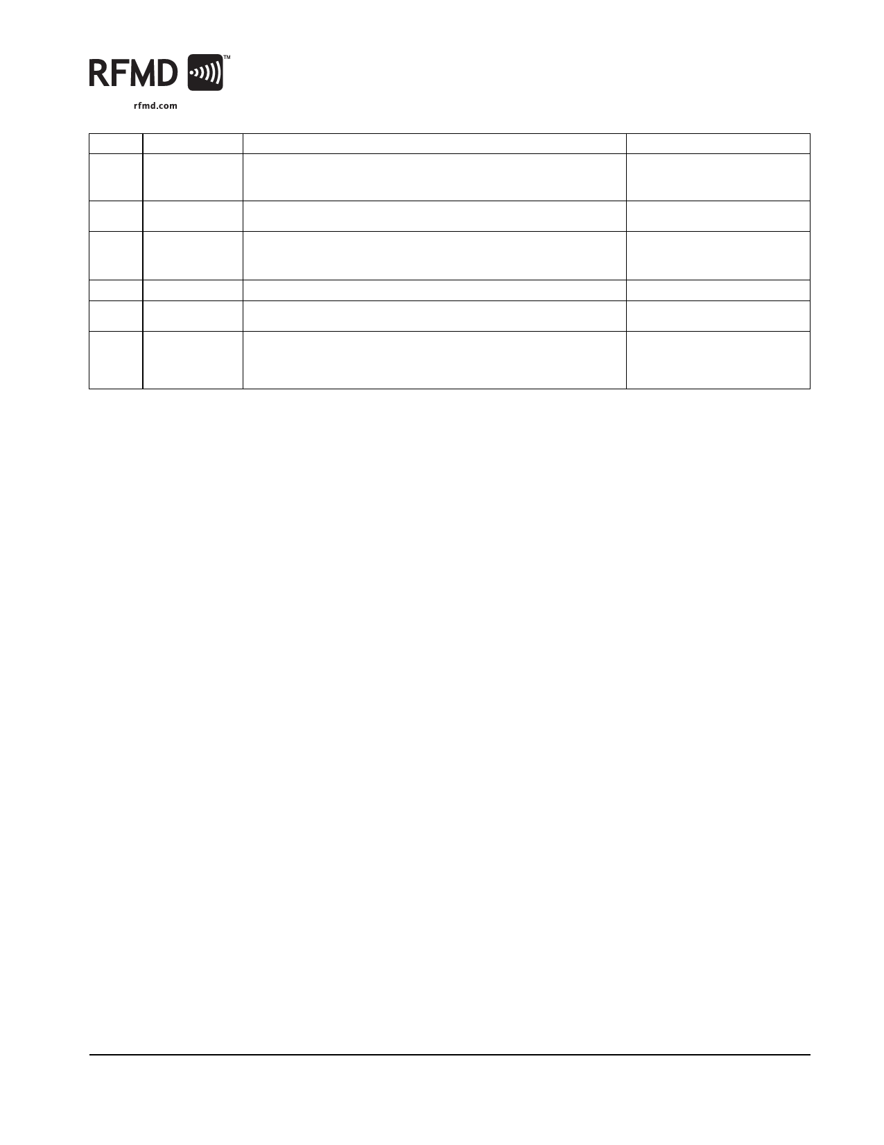
Pin Function Description
Interface Schematic
1
RF OUT
RF output pin. This pin is DC-coupled and requires VCC through a bias
inductor sized accordingly to provide a high pass transformation with a
series capacitor.
2
GND
Ground connection. For best performance, keep traces physically short
and connect immediately to ground plane.
3
GC
Analog gain control pin. This pin controls the gain of the IC. Minimum gain
occurs at VGC<0.4V and maximum gain is achieved with VGC=2.0V. 50dB
of linear gain control with little variation of input P1dB is available.
4
RF IN
RF input pin. This pin is DC-coupled.
5
GND
Ground connection. For best performance, keep traces physically short
and connect immediately to ground plane.
6
VCC
Power supply. This pin should be connected to a regulated supply and
requires a series inductor and bypass capacitor. Voltage is supplied
through this pin to the first stage collector; this voltage also controls the
bias. Gain may be tuned by adjusting the value of the feed inductor.
Package Drawing
Rev A2 DS060907
7628 Thorndike Road, Greensboro, NC 27409-9421 · For sales or technical
support, contact RFMD at (+1) 336-678-5570 or sales-support@rfmd.com.
5 of 10
Share Link: 