FDD3570 „Éá„Éľ„āŅ„ā∑„Éľ„Éą„ĀģŤ°®Á§ļÔľąPDFÔľČ - Fairchild Semiconductor
ťÉ®ŚďĀÁē™ŚŹ∑
„ā≥„É≥„ÉĚ„Éľ„Éć„É≥„ÉąŤ™¨śėé
„É°„Éľ„āę„Éľ
FDD3570 Datasheet PDF : 5 Pages
| |||
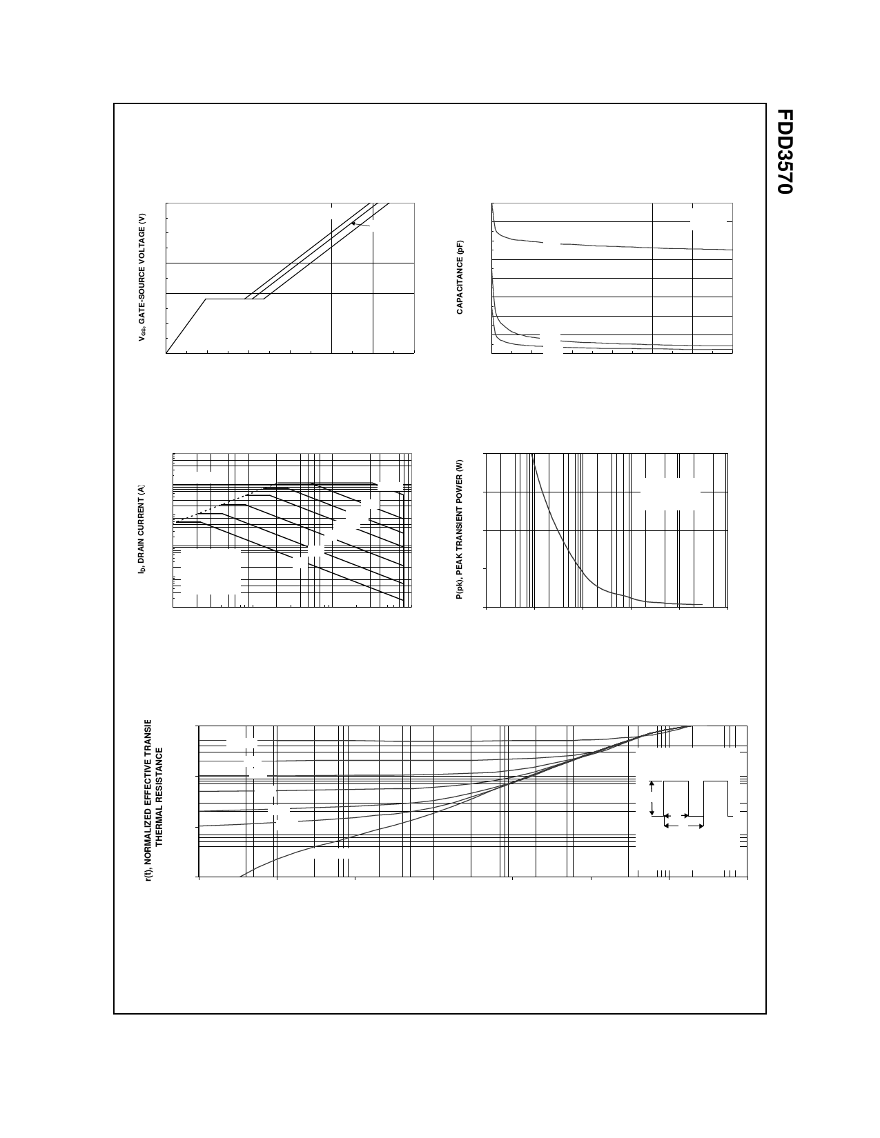
Typical Characteristics
10
ID = 9A
8
6
4
2
0
0
10
VDS = 10V
20V
40V
20
30
40
50
60
Qg, GATE CHARGE (nC)
Figure 7. Gate Charge Characteristics.
1000
RDS(ON) LIMIT
100
100¬Ķs
10
1
VGS = 10V
SINGLE PULSE
0.1
RőłJA = 96oC/W
TA = 25oC
1ms
10ms
100ms
1s
10s
DC
0.01
0.1
1
10
100
VDS, DRAIN-SOURCE VOLTAGE (V)
Figure 9. Maximum Safe Operating Area.
4000
3500
3000
2500
2000
1500
1000
500
0
0
f = 1MHz
VGS = 0 V
CISS
COSS
CRSS
10
20
30
40
50
60
VDS, DRAIN TO SOURCE VOLTAGE (V)
Figure 8. Capacitance Characteristics.
200
SINGLE PULSE
150
RőłJA = 96 ¬įC/W
TA = 25¬įC
100
50
0
0.01
0.1
1
10
t1, TIME (sec)
100
1000
Figure 10. Single Pulse Maximum
Power Dissipation.
1
0.1
0.01
D = 0.5
0.2
0.1
0.05
0.02
0.01
0.001
0.0001
0.001
SINGLE PULSE
0.01
0.1
1
t1, TIME (sec)
RőłJA(t) = r(t) + RőłJA
RőłJA = 96 ¬įC/W
P(pk)
t1
t2
TJ - TA = P * RőłJA(t)
Duty Cycle, D = t1 / t2
10
100
1000
Figure 11. Transient Thermal Response Curve.
Thermal characterization performed using the conditions described in Note 1c.
Transient thermal response will change depending on the circuit board design.
FDD3570 Rev. C(W)
Share Link: 