RMPA2271 データシートの表示(PDF) - Fairchild Semiconductor
部品番号
コンポーネント説明
メーカー
RMPA2271
Fairchild Semiconductor

RMPA2271 Datasheet PDF : 9 Pages
| |||
PRELIMINARY
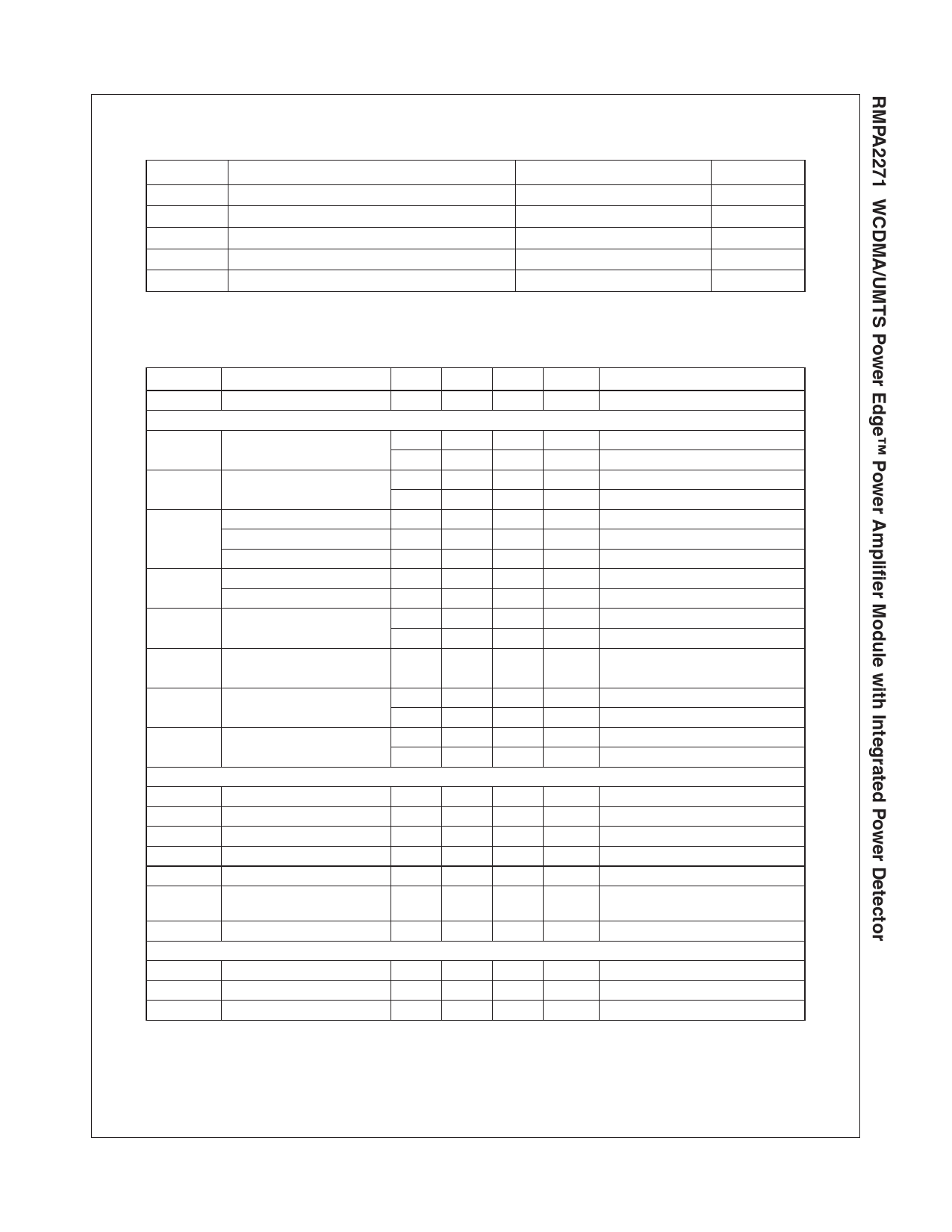
Absolute Ratings 1
Symbol
Parameter
Ratings
VCC1, VCC2
Vref
Vmode
PIN
TSTG
Supply Voltages
Reference Voltage
Power Control Voltage
RF Input Power
Storage Temperature
5.0
2.6 to 3.5
3.5
+10
-55 to +150
Note:
1. No permanent damage with only one parameter set at extreme limit. Other parameters set to typical values.
Electrical Characteristics (1920 to 1980 MHz)1
Units
V
V
V
dBm
°C
Symbol
Parameter
Min Typ Max Units
Comments
f
Operating Frequency
WCDMA Operation
Gp
Power Gain
Po
Linear Output Power
PAEd
Itot
Pdet
PAEd (digital) @ +28dBm
PAEd (digital) @ +16dBm
PAEd (digital) @ +16dBm
High Power Total Current
Low Power Total Current
Detector Output
Adjacent Channel Leakage
Ratio
1920
1980 MHz
27
26
28
16
41
9
25
450
130
1.4
0.3
dB
dB
dBm
dBm
%
%
%
mA
mA
V
V
Po = +28dBm, Vmode = 0V
Po = +16dBm, Vmode ≥ 2.0V
Vmode = 0V
Vmode ≥ 2.0V
Vmode = 0V
Vmode ≥ 2.0V
Vmode ≥ 2.0V, Vcc = 1.4V
Po = +28dBm, Vmode = 0V
Po = +16dBm, Vmode ≥ 2.0V
Po = +28dBm, Vmode = 0V
Po = +16dBm, Vmode ≥ 2.0V
WCDMA Modulation 3GPP
3.2 03-00 DPCCH+1 DCDCH
ACLR1
±5.00MHz Offset
1920–1980MHz
ACLR2
±10.00MHz Offset
1920–1980MHz
General Characteristics
VSWR
Input Impedance
NF
Noise Figure
Rx No
2fo – 5fo
S
Receive Band Noise Power
Harmonic Suppression3
Spurious Outputs2, 3
Ruggedness with Load
Mismatch 3
Tc
Case Operating Temperature -30
DC Characteristics
Iccq
Quiescent Current
Iref
Reference Current
Icc(off)
Shutdown Leakage Current
-40
dBc Po = +28dBm, Vmode = 0V
-42
dBc Po = +16dBm, Vmode ≥ 2.0V
-54
dBc Po = +28dBm, Vmode = 0V
-66
dBc Po = +16dBm, Vmode ≥ 2.0V
2.0:1
4
-142
dB
dBm/Hz Po ≤ +28dBm, 2110 to 2170MHz
-50
dBc Po ≤ +28dBm
-60
dBc Load VSWR ≤ 5.0:1
10:1
No permanent damage
85
°C
50
mA Vmode ≥ 2.0V
7
mA Po ≤ +28dBm
1
5
µA No applied RF signal
Notes:
1. All parameters met at TC = +25°C, VCC = +3.4V, Vref = 2.85V and load VSWR ≤ 1.2:1, unless otherwise noted.
RMPA2271 Rev. B
2
www.fairchildsemi.com
Share Link: