NJU6677 データシートの表示(PDF) - Japan Radio Corporation
部品番号
コンポーネント説明
メーカー
NJU6677 Datasheet PDF : 45 Pages
| |||
NJU6677
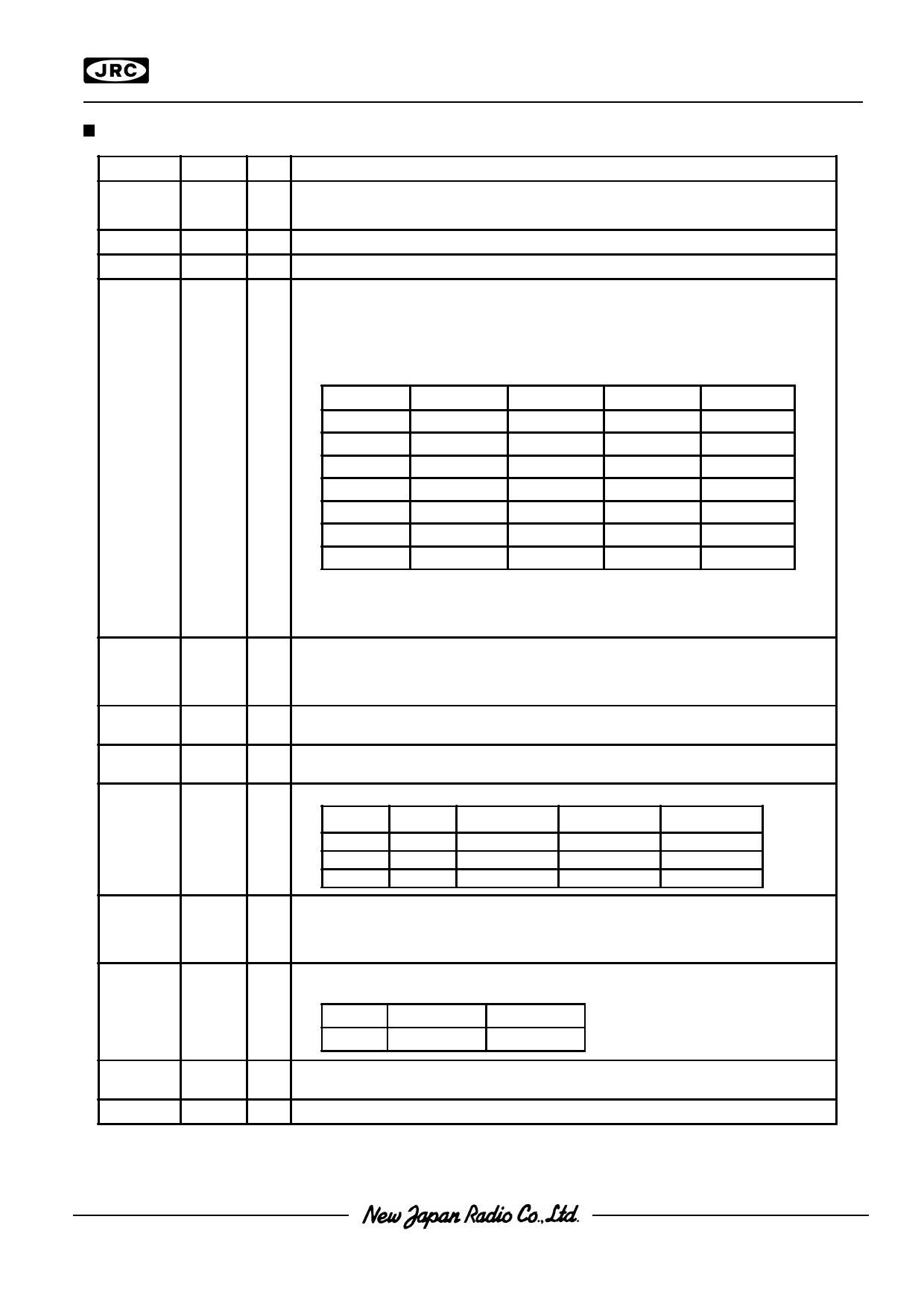
TERMINAL DESCRIPTION
No.
Symbol I/O
Function
1,41 to 44 DUMMY0
to
DUMMY4
Dummy Terminals.
These terminals are insulated.
2,33,40 VDD
Power VDD=+3V
6,23
VSS
GND VSS=0V
39,
V1
Power LCD Driving Voltage Supplying Terminal. When the internal voltage booster is
38,
V2
not used, supply each level of LCD driving voltage from outside with following
37,
V3
relation.
36,
V4
35
V5
WheVnDthDe>=iVn1te>=rnVa2l>=pVo3w>=eVr 4s>=uVpp5ly is on, the internal circuits generate and supply
following LCD bias voltage from V1 to V4 terminals.
Bias
1/4Bias
1/5Bias
1/6Bias
1/7Bias
1/8Bias
1/9Bias
1/10Bias
V1
V5+3/4VLCD
V5+4/5VLCD
V5+5/6VLCD
V5+6/7VLCD
V5+7/8VLCD
V5+8/9VLCD
V5+9/10VLCD
V2
V5+2/4VLCD
V5+3/5VLCD
V5+4/6VLCD
V5+5/7VLCD
V5+6/8VLCD
V5+7/9VLCD
V5+8/10VLCD
V3
V5+2/4VLCD
V5+2/5VLCD
V5+2/6VLCD
V5+2/7VLCD
V5+2/8VLCD
V5+2/9VLCD
V5+2/10VLCD
V4
V5+1/4VLCD
V5+1/5VLCD
V5+1/6VLCD
V5+1/7VLCD
V5+1/8VLCD
V5+1/9VLCD
V5+1/10VLCD
31,32,
29,30,
27,28,
25,26
24
34
8,
7
15 to 22
12
5
11
C1+,C1-
C2+,C2-
C3+,C3-
C4+,C4-
VOUT
VR
T1
T2
D0 to
D7
(SI)
(SCL)
A0
RES
CS
(V L C D =V D D -V 5)
O Step up capacitor connecting terminals.
Voltage booster circuit (Maximum 5-time)
O Step up voltage output terminal. Connect the step up capacitor between this
terminal and VSS.
I Voltage adjust terminal. V5 level is adjusted by external bleeder resistance
connecting between VDD and V5 terminal.
I LCD bias voltage control terminals. ( *:Don't Care)
T1
T2
Volta g e
b o o s ter C ir.
Volta g e A d j.
L
*
A v a ila b le
A v a ila b le
H
L
N o t Avail.
A v a ila b le
H
H
N o t Avail.
N o t Avail.
V /F C ir.
A v a ila b le
A v a ila b le
A v a ila b le
I/O P/S="H" : Tri-state bi-directional Data I/O terminal in 8-bit parallel operation.
P/S="L" : D7=Serial data input terminal. D 6=Serial data clock signal input
terminal. Data from SI is loaded at the rising edge of SCL and
latched as the parallel data at 8th rising edge of SCL.
I Connect to the Address bus of MPU. The data on the D 0 to D7 is
distinguished between Display data and Instruction by status of A0.
A0
H
L
Distin. Display Data Instruction
I Reset terminal. When the RES terminal goes to "L", the initialization is
performed. Reset operation is executing during "L" state of RES.
I Chip select terminal. Data Input/Output are available during CS ="L".
Share Link: 