STK1743-D35I データシートの表示(PDF) - Simtek Corporation
部品番号
コンポーネント説明
メーカー
STK1743-D35I Datasheet PDF : 10 Pages
| |||
STK1743
DEVICE OPERATION
The STK1743 is an 8K x 8 nonvolatile static RAM
with a full-function real-time clock (RTC). The data
integrity is secured in EEPROM, not subject to bat-
tery or capacitor discharge. The real-time clock reg-
isters reside in the eight uppermost RAM locations,
and contain century, year, month, date, day, hour,
minute and second data in 24-hour BCD format. Cor-
rections for the day of the month and leap years are
made automatically. This nonvolatile time-keeping
RAM is functionally similar to any JEDEC standard
8K x 8 SRAM.
The RTC registers are double-buffered to avoid
access of incorrect data that could otherwise occur
during clock update cycles. The double-buffered
system prevents time loss by maintaining internal
clock operation while time register data is accessed.
The STK1743 contains integral power-fail circuitry
that deselects the device when VCC drops below
VSWITCH.
The STK1743 is a pin-compatible replacement for
the ST Microelectronics M48T08 and the Dallas
Semiconductor DS1743, but without the limitations
of an embedded lithium battery. The Simtek device
uses a double-layer high-value capacitor to maintain
RTC operation on power down for at least 30 days.
The part can be soldered directly onto printed circuit
boards and handled without concern for damaging
or discharging internal batteries. Unlike some other
RTCs, the STK1743 is Year 2000-compliant.
NOISE CONSIDERATIONS
Note that the STK1743 is a high-speed memory and
so must have a high-frequency bypass capacitor of
approximately 0.1µF connected between VCC and
VSS, using leads and traces that are as short as pos-
sible. As with all high-speed CMOS ICs, normal care-
ful routing of power, ground and signals will help
prevent noise problems.
SRAM AND RTC READ
The STK1743 performs a READ cycle whenever E
and G are low and W is high. The address specified
on pins A0-12 determines which of the 8,192 data
bytes will be accessed. When the READ is initiated
by an address transition, the outputs will be valid
after a delay of tAVQV (READ cycle #1). If the READ is
initiated by E or G, the outputs will be valid at tELQV or
at tGLQV, whichever is later (READ cycle #2). The data
outputs will repeatedly respond to address changes
within the tAVQV access time without the need for tran-
sitions on any control input pins, and will remain valid
until another address change or until E or G is
brought high or W is brought low.
Note that the eight most significant bytes of the
address space are reserved for accessing the RTC
registers, as shown in the Register Map below.
While the double-buffered RTC register structure
reduces the chance of reading incorrect data from the
clock, the user should halt internal updates to the
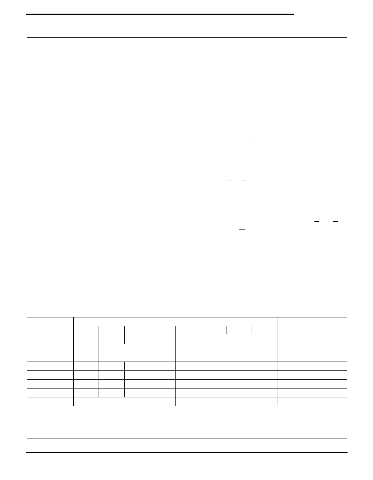
RTC REGISTER MAP
ADDRESS
BCD DATA
(HEXADECIMAL)
D7
D6
D5
D4
D3
1FF8
W
R
10 Centuries
1FF9
X
10 Seconds
1FFA
X
10 Minutes
1FFB
X
X
10 Hours
1FFC
1
FT
X
X
X
1FFD
X
X
10 Dates
1FFE
X
X
X
10 Mos.
1FFF
10 Years
Key:
R = Read Bit
W = Write Bit
1 = Battery Flag High (no battery to fail)
FT = Frequency Test Bit
X = Don’t Care
D2
D1
Centuries
Seconds
Minutes
Hours
Days
Dates
Months
Years
FUNCTION/RANGE
D0
Centuries: 00-39, Control
Seconds: 00 - 59
Minutes: 00 - 59
Hours: 00 - 23
Days: 01 - 07
Dates: 01 - 31
Months: 01 - 12
Years: 00 - 99
March 1999
7-7
Share Link: 