STK1743-D35I データシートの表示(PDF) - Simtek Corporation
部品番号
コンポーネント説明
メーカー
STK1743-D35I Datasheet PDF : 10 Pages
| |||
1. Read address
2. Read address
3. Read address
4. Read address
5. Read address
6. Read address
0000 (hex)
1555 (hex)
0AAA (hex)
1FFF (hex)
10F0 (hex)
0F0E (hex)
Valid READ
Valid READ
Valid READ
Valid READ
Valid READ
Initiate RECALL cycle
Internally, RECALL is a two-step procedure. First,
the SRAM data is cleared, and second, the nonvola-
tile information is transferred into the SRAM cells.
After the tRECALL cycle time the SRAM will once again
be ready for READ and WRITE operations. The
RECALL operation in no way alters the data in the
EEPROM cells. The nonvolatile data can be recalled
an unlimited number of times. Note that the RTC
registers are not affected by nonvolatile operations.
AutoStoreTM OPERATION
The STK1743 uses capacitance built into the mod-
ule to perform an automatic STORE on power down.
In order to prevent unnecessary STORE operations,
automatic STOREs will be ignored unless at least
one WRITE operation has taken place since the
most recent STORE or RECALL cycle. Software-
initiated STORE cycles are performed regardless of
whether a WRITE operation has taken place.
POWER-UP RECALL
During power up, or after any low-power condition
(VCC < VRESET), an internal recall request will be
STK1743
latched. When VCC once again exceeds VSWITCH, a
RECALL cycle will automatically be initiated and will
take tRESTORE to complete.
HARDWARE PROTECT
The STK1743 offers hardware protection against
inadvertent STORE and SRAM WRITE operation dur-
ing low-voltage conditions. When VCC < VSWITCH, all
software STORE operations and SRAM writes are
inhibited.
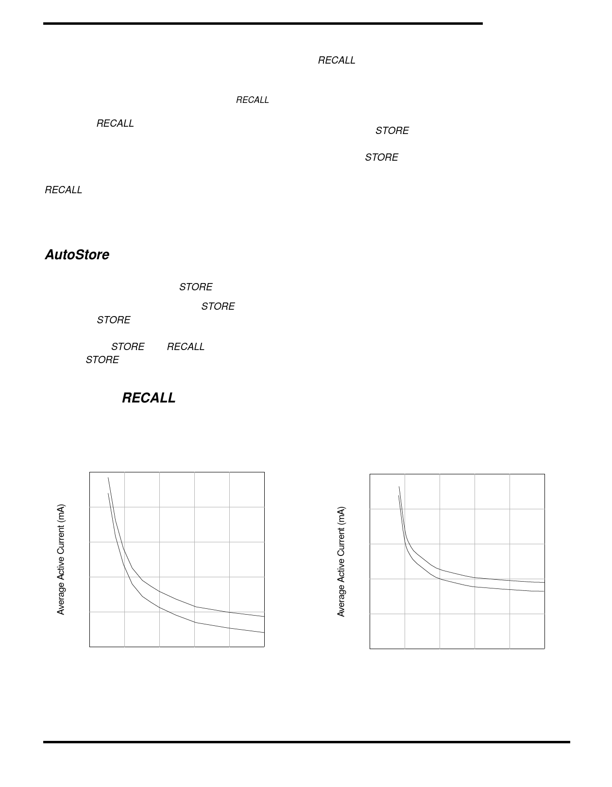
LOW AVERAGE ACTIVE POWER
The STK1743 draws significantly less current when
it is cycled at times longer than 50ns. Figure 2
shows the relationship between ICC and READ cycle
time. Worst-case current consumption is shown for
both CMOS and TTL input levels (commercial tem-
perature range, VCC = 5.5V, 100% duty cycle on chip
enable). Figure 3 shows the same relationship for
WRITE cycles. If the chip enable duty cycle is less
than 100%, only standby current is drawn when the
chip is disabled. The overall average current drawn
by the STK1743 depends on the following items:
1) CMOS vs. TTL input levels; 2) the duty cycle of
chip enable; 3) the overall cycle rate for accesses;
4) the ratio of READs to WRITEs; 5) the operating
temperature; 6) the VCC level; and 7) I/O loading.
100
80
60
40
TTL
20
CMOS
0
50
100 150 200
Cycle Time (ns)
Figure 2: ICC (max) Reads
100
80
60
TTL
40
CMOS
20
0
50
100 150 200
Cycle Time (ns)
Figure 3: ICC (max) Writes
March 1999
7-9
Share Link: 