CY7C4241-10JI データシートの表示(PDF) - Cypress Semiconductor
部品番号
コンポーネント説明
メーカー
CY7C4241-10JI Datasheet PDF : 20 Pages
| |||
CY7C4421/4201/4211/4221
CY7C4231/4241/4251
Programmable Flag (PAE, PAF) Operation
Whether the flag offset registers are programmed as described
in Table 2 or the default values are used, the programmable
almost-empty flag (PAE) and programmable almost-full flag
(PAF) states are determined by their corresponding offset
registers and the difference between the read and write pointers.
The number formed by the empty offset least significant bit
register and empty offset most significant register is referred to
as n and determines the operation of PAE. PAE is synchronized
to the LOW-to-HIGH transition of RCLK by one flip-flop and is
LOW when the FIFO contains n or fewer unread words. PAE is
set HIGH by the LOW-to-HIGH transition of RCLK when the
FIFO contains (n + 1) or greater unread words.
The number formed by the full offset least significant bit register
and full offset most significant bit register is referred to as m and
determines the operation of PAF. PAE is synchronized to the
LOW-to-HIGH transition of WCLK by one flip-flop and is set LOW
when the number of unread words in the FIFO is greater than or
equal to CY7C4421. (64 – m), CY7C4201 (256 – m), CY7C4211
(512 – m), CY7C4221 (1K – m), CY7C4231 (2K – m),
CY7C4241 (4K – m), and CY7C4251 (8K – m). PAF is set HIGH
by the LOW-to-HIGH transition of WCLK when the number of
available memory locations is greater than m.
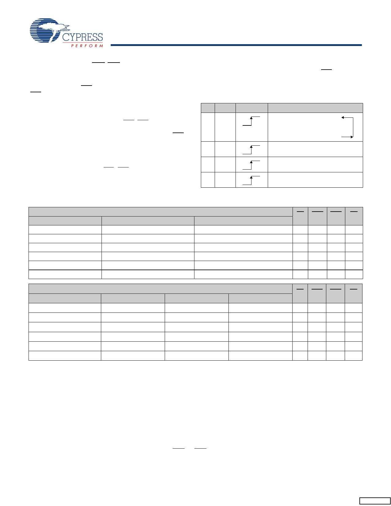
Table 2. Writing the Offset Registers
LD WEN WCLK[1]
Selection
00
Empty Offset (LSB)
Empty Offset (MSB)
Full Offset (LSB)
Full Offset (MSB)
01
No Operation
10
Write Into FIFO
11
No Operation
Table 3. Status Flags
CY7C4421
0
1 to n[2]
(n + 1) to 32
33 to (64 – (m + 1))
(64 – m)[3] to 63
64
Number of Words in FIFO
CY7C4201
CY7C4211
0
1 to n[2]
0
1 to n[2]
(n + 1) to 128
(n + 1) to 256
129 to (256 – (m + 1))
(256 – m)[3] to 255
257 to (512 – (m + 1))
(512 – m)[3] to 511
256
512
FF PAF PAE EF
HH
L
L
HH
L
H
HH H H
HH H H
HL HH
LL HH
CY7C4221
0
1 to n[2]
(n + 1) to 512
513 to (1024 – (m + 1))
(1024 – m)[3] to 1023
1024
Number of Words in FIFO
CY7C4231
CY7C4241
CY7C4251
FF PAF PAE EF
0
1 to n[2]
0
1 to n[2]
0
1 to n[2]
HH
L
L
HH
L
H
(n + 1) to 1024
(n + 1) to 2048
(n + 1) to 4096
HH H H
1025 to (2048 – (m + 1)) 2049 to (4096 – (m + 1)) 4097 to (8192 – (m + 1)) H H H H
(2048 – m)[3] to 2047 (4096 – m)[3] to 4095 (8192 – m)[3] to 8191
HL H H
2048
4096
8192
LL HH
Notes
1. The same selection sequence applies to reading from the registers. REN1 and REN2 are enabled and a read is performed on the LOW-to-HIGH transition of RCLK.
2. n = Empty Offset (n = 7 default value).
3. m = Full Offset (m = 7 default value).
Document #: 38-06016 Rev. *D
Page 7 of 20
[+] Feedback
Share Link: 