CY7C4241-10JI データシートの表示(PDF) - Cypress Semiconductor
部品番号
コンポーネント説明
メーカー
CY7C4241-10JI Datasheet PDF : 20 Pages
| |||
CY7C4421/4201/4211/4221
CY7C4231/4241/4251
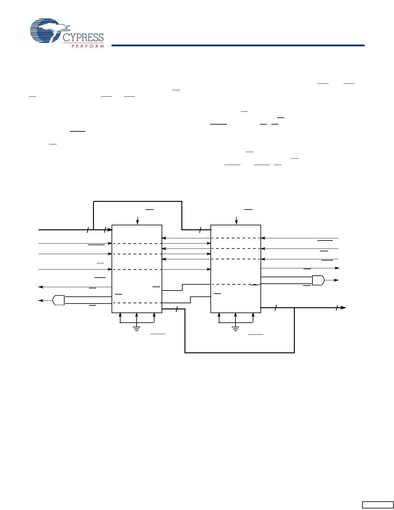
Width Expansion Configuration
Flag Operation
Word width may be increased by connecting the corresponding
input controls signals of multiple devices. A composite flag
should be created for each of the end-point status flags (EF and
FF). The partial status flags (PAE and PAF) can be detected from
any one device. Figure 3 demonstrates a 18-bit word width by
using two CY7C42X1s. Any word width can be attained by
adding additional CY7C42X1s.
When the CY7C42X1 is in a Width Expansion Configuration, the
Read Enable (REN2) control input can be grounded (See
Figure 3). In this configuration, the Write Enable 2/Load
(WEN2/LD) pin is set to LOW at Reset so that the pin operates
as a control to load and read the programmable flag offsets.
The CY7C42X1 devices provide four flag pins to indicate the
condition of the FIFO contents. Empty, Full, PAE, and PAF are
synchronous.
Full Flag
The Full Flag (FF) goes LOW when device is full. Write opera-
tions are inhibited whenever FF is LOW regardless of the state
of WEN1 and WEN2/LD. FF is synchronized to WCLK - it is
exclusively updated by each rising edge of WCLK.
Empty Flag
The Empty Flag (EF) goes LOW when the device is empty. Read
operations are inhibited whenever EF is LOW, regardless of the
state of REN1 and REN2. EF is synchronized to RCLK - it is
exclusively updated by each rising edge of RCLK.
Figure 3. Block Diagram of 64 x 9, 256 x 9, 512 x 9, 1024 x 9, 2048 x 9, 4096 x 9, 8192 x 9 Synchronous FIFO Memory Used
in a Width Expansion Configuration
RESET (RS)
DATA IN (D) 18 9
Write CLOCK (WCLK)
Write ENABLE 1 (WEN1)
Write ENABLE 2/LOAD
(WEN2/LD)
PROGRAMMABLE (PAF)
CY7C42X1
FULL FLAG (FF) # 1
EF
FF
FULL FLAG (FF) # 2
9
RESET (RS)
9
Read CLOCK (RCLK)
CY7C42X1
Read ENABLE 1 (REN1)
OUTPUT ENABLE (OE)
PROGRAMMABLE (PAE)
EMPTY FLAG (EF) #1
EF EMPTY FLAG (EF) #2
FF
9 DATA OUT (Q) 18
Read Enable 2 (REN2)
Read Enable 2 (REN2)
Document #: 38-06016 Rev. *D
Page 8 of 20
[+] Feedback
Share Link: 