CY7C185-15VI(2001) データシートの表示(PDF) - Cypress Semiconductor
部品番号
コンポーネント説明
メーカー
CY7C185-15VI Datasheet PDF : 11 Pages
| |||
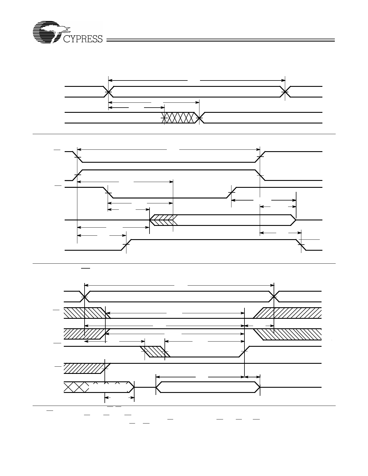
Switching Waveforms
Read Cycle No.1[9,10]
tRC
ADDRESS
DATA OUT
tAA
tOHA
PREVIOUS DATA VALID
Read Cycle No.2[11,12]
CE1
tRC
CY7C185
DATA VALID
C185–6
CE2
OOEE
DATA OUT
VCC
SUPPLY
CURRENT
tACE
tDOE
tLZOE
HIGH IMPEDANCE
tLZCE
tPU
50%
DATA VALID
Write Cycle No. 1 (WE Controlled)[10,12]
ADDRESS
CE1
CCEE2
tSA
WE
tWC
tSCEI
tAW
tSCE2
tPWE
tHZOE
tHZCE
HIGH
IMPEDANCE
tPD
50%
ICC
ISB
C185–7
tHA
OE
DATA I/O
NOTE 13
tHZOE
tSD
DATA IN VALID
tHD
C185–8
9. Device is continuously selected. OE, CE1 = VIL. CE2 = VIH.
10. WE is HIGH for read cycle.
11. Data I/O is High Z if OE = VIH, CE1 = VIH, WE = VIL, or CE2=VIL.
12. The internal write time of the memory is defined by the overlap of CE1 LOW, CE2 HIGH and WE LOW. CE1 and WE must be LOW and CE2 must be HIGH
to initiate write. A write can be terminated by CE1 or WE going HIGH or CE2 going LOW. The data input set-up and hold timing should be referenced to the
rising edge of the signal that terminates the write.
13. During this period, the I/Os are in the output state and input signals should not be applied.
Document #: 38-05043 Rev. **
Page 5 of 11
Share Link: 