RT8287A データシートの表示(PDF) - Richtek Technology
部品番号
コンポーネント説明
メーカー
RT8287A Datasheet PDF : 14 Pages
| |||
Application Information
The IC is a synchronous high voltage buck converter that
can support the input voltage range from 4.5V to 21V and
the output current can be up to 4A.
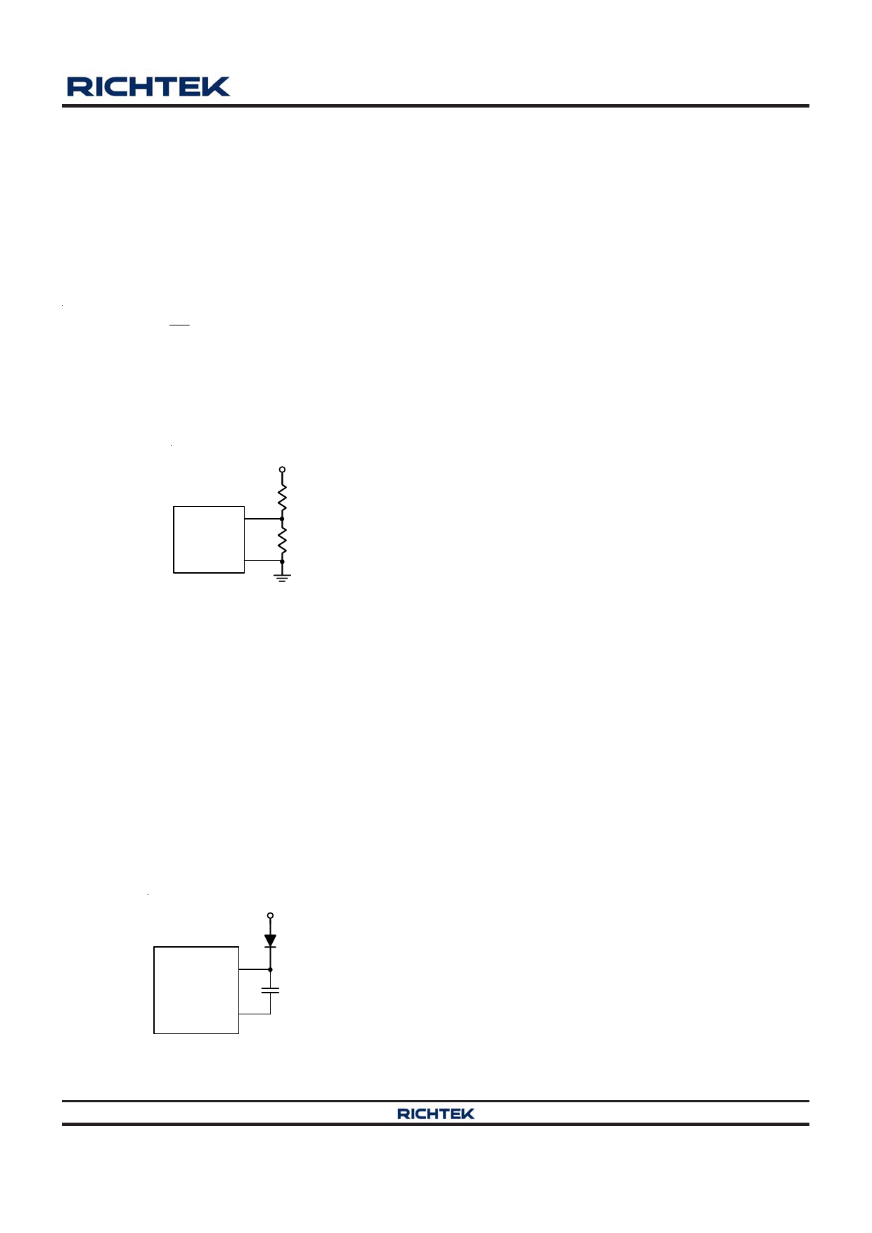
Output Voltage Setting
The output voltage is set by an external resistive divider
according to the following equation :
VOUT
=
VFB
⎛⎜⎝1+
R1
R2
⎞⎟⎠
where VFB is the feedback reference voltage 0.808V
(typical).
The resistive divider allows the FB pin to sense a fraction
of the output voltage as shown in Figure 1.
VOUT
R1
FB
RT8287A
R2
GND
Figure 1. Output Voltage Setting
External Bootstrap Diode
Connect a 100nF low ESR ceramic capacitor between
the BOOT pin and SW pin as shown in Figure 2. This
capacitor provides the gate driver voltage for the high side
MOSFET. It is recommended to add an external bootstrap
diode between an external 5V and BOOT pin for efficiency
improvement when input voltage is lower than 5.5V or duty
ratio is higher than 65% .The bootstrap diode can be a
low cost one such as IN4148 or BAT54. The external 5V
can be a 5V fixed input from system or a 5V output of the
IC. Note that the external boot voltage must be lower than
5.5V.
5V
BOOT
RT8287A
SW
100nF
Figure 2. External Bootstrap Diode
RT8287A
Soft-Start
The IC contains an external soft-start clamp that gradually
raises the output voltage. The soft-start timing is
programmed by the external capacitor between SS pin
and GND. The chip provides an internal 10μA charge current
for the external capacitor. If 47nF capacitor is used to set
the soft-start, the period will be 4.7ms (typ.).
Under Voltage Lockout Threshold
The IC includes an input Under Voltage Lockout Protection
(UVLO). If the input voltage exceeds the UVLO rising
threshold voltage (4.2V), the converter resets and prepares
the PWM for operation. If the input voltage falls below the
UVLO falling threshold voltage (3.8V) during normal
operation, the device stops switching. The UVLO rising
and falling threshold voltage includes a hysteresis to
prevent noise caused reset.
Chip Enable Operation
The EN pin is the chip enable input. Pulling the EN pin
low (<0.4V) will shut down the device. During shutdown
mode, the IC quiescent current drops to lower than 1μA.
Driving the EN pin high (>2V, <5.5V) will turn on the device
again. For external timing control (e.g.RC), the EN pin
can also be externally pulled high by adding a REN* resistor
and CEN* capacitor from the VIN pin, as can be seen from
the Figure 5.
An external MOSFET can be added to implement digital
control on the EN pin when front age system voltage below
2.5V is available, as shown in Figure 3. In this case, a
100kΩ pull-up resistor, REN, is connected between VIN
and the EN pin. MOSFET Q1 will be under logic control to
pull down the EN pin.
To prevent enabling circuit when VIN is smaller than the
VOUT target value, a resistive voltage divider can be placed
between the input voltage and ground and connected to
the EN pin to adjust IC lockout threshold, as shown in
Figure 4. For example, if an 8V output voltage is regulated
from a 12V input voltage, the resistor REN2 can be selected
to set input lockout threshold larger than 8V.
Copyright ©2012 Richtek Technology Corporation. All rights reserved.
DS8287A-03 June 2012
is a registered trademark of Richtek Technology Corporation.
www.richtek.com
9
Share Link: 