ID242 データシートの表示(PDF) - Sharp Electronics
部品番号
コンポーネント説明
メーカー
ID242 Datasheet PDF : 33 Pages
| |||
SHARP
ID242 SERIES PRODUCT OVERVIEW
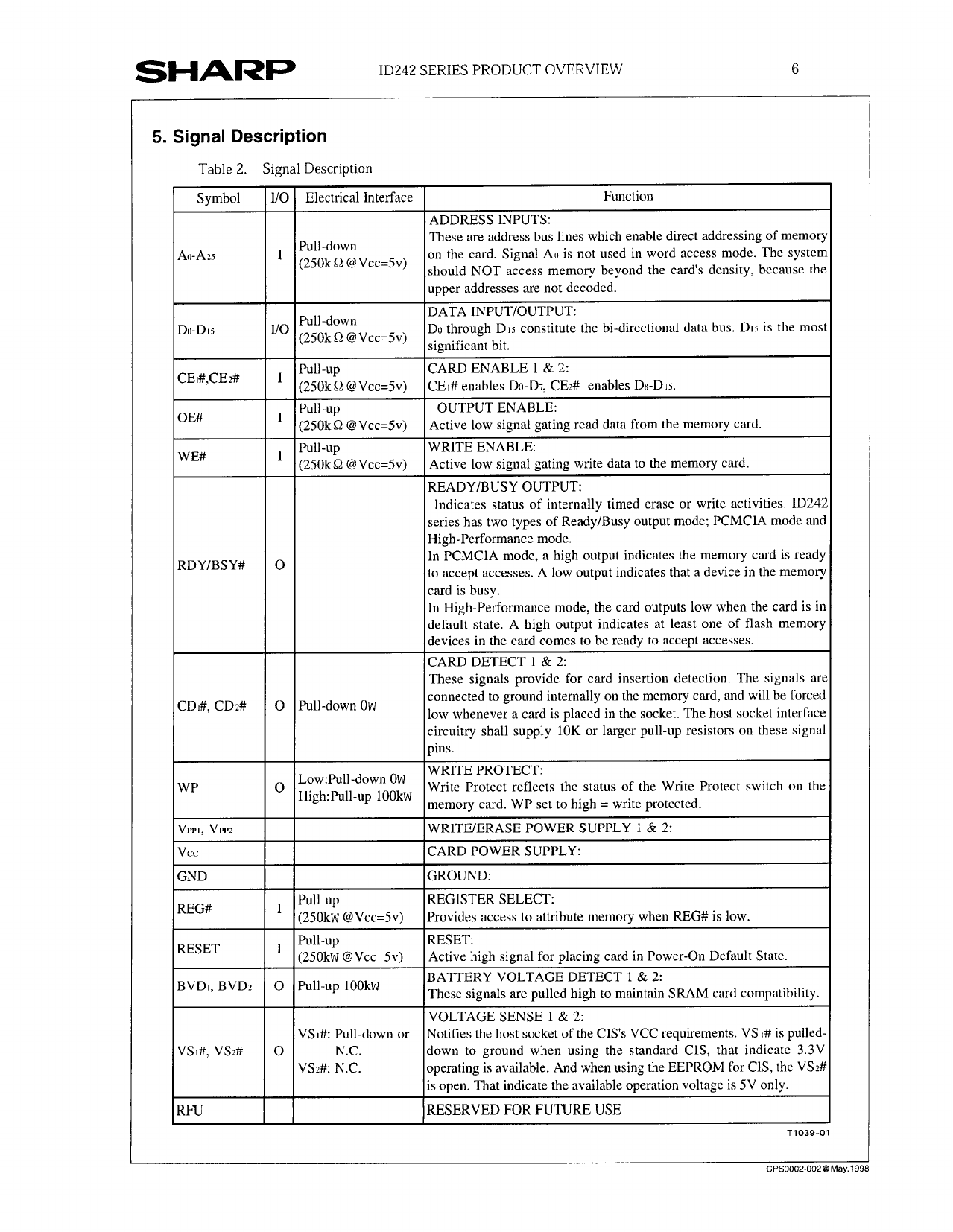
5. Signal Description
Table 2. Signal Description
Symbol l/O Electrical interface
Ao-Azs
1 Pull-down
(250k Q @ Vcc=Sv)
Du-D15
1/o Pull-down
(2’0k ’ @VCC=‘V)
Function
ADDRESS INPUTS:
These are address bus lines which enable direct addressing of memory
on the card. Signal AI) is not used in word access mode. The system
should NOT access memory beyond the card’s density. because the
upper addresses are not decoded.
DATA INPUT/OUTPUT:
De through Dls constitute the bi-directional data bus. DIG is the most
significant bit,
CEI#,CEZ#
OE#
WE#
RDY/BSY#
CDt#, CD2#
WP
VPPI, VW2
vcc
GND
REG#
RESET
BVDt, BVD2
VSI#, VS2#
RFU
1 Pull-up
(250k Q @Vcc=Sv)
1 Pull-up
(250k Q @ Vcc=Sv)
CARD ENABLE I & 2:
CEI# enables Do-D7, CE2# enables Dx-DIG.
OUTPUT ENABLE:
Active low signal gating read data from the memory card.
1 Pull-up
WRlTE ENABLE:
(250k 52@ Vcc=Sv) Active low signal gating write data to the memory c‘ard.
0
0 Pull-down Ow
READY/BUSY OUTPUT:
indicates status of internally timed erase or write activities. lD242
series has two types of Ready/Busy output mode; PCMClA mode and
High-Performance mode.
In PCMClA mode, a high output indicates the memory card is ready
to accept accesses. A low output indicates that a device in the memory
c,ard is busy.
In High-Performance mode, the card outputs low when the card is in
default state. A high output indicates at least one of flash memory
devices in the card comes to be ready to accept accesses.
CARD DETECT 1 & 2:
These signals provide for card insertion detection. The signals are
connected to ground internally on the memory card, and will be forced
low whenever a card is placed in the socket. The host socket interface
circuitry shall supply 10K or larger pull-up resistors on these signal
pins.
o
LowPull-down
High:Pull-up
OW
1OOkw
WRlTE PROTECT:
Write Protect reflects the status of the Write Protect switch on the
memory card. WP set to high = write protected.
WRITE/ERASE POWER SUPPLY 1 & 2:
CARD POWER SUPPLY:
GROUND:
1 Pull-up
(250kw @Vcc=Sv)
REGlSTER SELECT:
Provides access to attribute memory when REG# is low.
1 Pull-up
(250kw @Vcc=Sv)
0 Pull-up 1OOkw
RESET:
Active high signal for placing card in Power-On Default State.
BATTERY VOLTAGE DETECT 1 & 2:
These signals are pulled high to maintain SRAM card compatibility.
VOLTAGE SENSE 1 & 2:
VSI#: Pull-down or Notifies the host socket of the ClS’s VCC requirements. VS I# is pulled-
0
N.C.
down to ground when using the standard ClS, that indicate 3.3V
VSB: N.C.
operating is available. And when using the EEPROM for ClS, the VS2#
is open. That indicate the available operation voltage is 5V only.
RESERVED FOR FUTURE USE
CPSOOOZ-002@Mav.1991
Share Link: 