RT9187 データシートの表示(PDF) - Richtek Technology
部品番号
コンポーネント説明
メーカー
RT9187 Datasheet PDF : 9 Pages
| |||
RT9187
Absolute Maximum Ratings (Note 1)
Supply Input Voltage -------------------------------------------------------------------------------------------------- 6V
EN Input Voltage ------------------------------------------------------------------------------------------------------- 6V
Power Dissipation, PD @ TA = 25°C
VDFN-8L 3x3 ----------------------------------------------------------------------------------------------------------- 0.923W
SOP-8 (Exposed Pad) ----------------------------------------------------------------------------------------------- 1.33W
Package Thermal Resistance (Note 9)
VDFN-8L 3x3, θJC ----------------------------------------------------------------------------------------------------- 8.2°C/W
VDFN-8L 3x3, θJA ------------------------------------------------------------------------------------------------------ 108°C/W
SOP-8 (Exposed Pad), θJC ----------------------------------------------------------------------------------------- 15°C/W
SOP-8 (Exposed Pad)-8, θJA --------------------------------------------------------------------------------------- 75°C/W
Lead Temperature (Soldering, 10 sec.) --------------------------------------------------------------------------- 260°C
Junction Temperature ------------------------------------------------------------------------------------------------- 150°C
Storage Temperature Range ---------------------------------------------------------------------------------------- −65°C to 150°C
ESD Susceptibility (Note 2)
HBM ---------------------------------------------------------------------------------------------------------------------- 2kV
MM ------------------------------------------------------------------------------------------------------------------------ 200V
Recommended Operating Conditions (Note 3)
Supply Input Voltage -------------------------------------------------------------------------------------------------- 2.5V to 5.5V
EN Input Voltage ------------------------------------------------------------------------------------------------------- 0V to 5.5V
Junction Temperature Range ---------------------------------------------------------------------------------------- −40°C to 125°C
Ambient Temperature Range ---------------------------------------------------------------------------------------- −40°C to 85°C
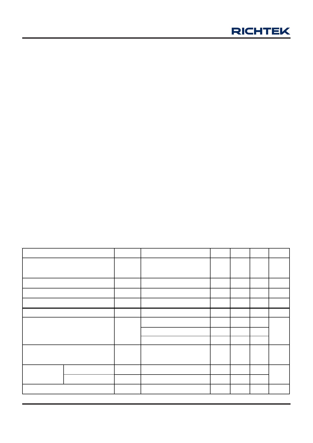
Electrical Characteristics
(VIN = VOUT + 1V, VEN = VIN, CIN = COUT = 2.2μF (Ceramic) & CBP = 10nF, TA = 25°C unless otherwise specified)
Pa rame te r
Symbol
Test Conditions
Min Typ Max
Units
Output Voltage Accuracy
(Fixed Output Voltage)
ΔVOUT IO UT = 10mA
−2
0
+2
%
Output Voltage Range (Adjustable)
Quiescent Current (Note 6)
Standby Current (Note 7)
Current Limit
Dropout Voltage (Note 4)
Load Regulation (Note 5)
(Fixed Output Voltage)
V OUT _Adj
IQ
VEN ≥ VIH, IOUT = 0mA
IS TBY
VEN ≤ VIL,VIN = 3.3V
ILIM
RLOAD = 0.5Ω, VIN = 3.3V
V DR OP
IOUT = 0.25A (N ote 8)
IOUT = 0.5A
IOUT = 1.0A
ΔVLOAD
VIN = (VOUT + 0.5V)
10mA < IOUT < 1.0A
EN Threshold
Logic-Low Voltage VIL
Logic-High Voltage VIH
Enable Pin Current
IE N
VIN = 3.3V
VIN = 3.3V
VIN = 3.3V, Enable
www.richtek.com
4
0.8
--
4.5
V
--
380 500 μA
--
0.1
1
μA
2
2.8
3
A
--
60 100
--
120 180 mV
--
240 360
--
0.4
-- %/A
--
--
0.6
V
1.8
--
--
--
0.1
1
μA
To be continued
DS9187-09 April 2008
Share Link: 