RT9205GS データシートの表示(PDF) - Richtek Technology
部品番号
コンポーネント説明
メーカー
RT9205GS Datasheet PDF : 15 Pages
| |||
RT9205/A
Preliminary
Absolute Maximum Ratings
l Supply Voltage VCC ------------------------------------------------------------------------------------------------ 7V
l BOOT & UGATE to GND ------------------------------------------------------------------------------------------- 19V
l Input, Output or I/O Voltage --------------------------------------------------------------------------------------- GND-0.3V to 7V
l Package Thermal Resistance
SOP-14, θJA ----------------------------------------------------------------------------------------------------------------------------------------------------- 160° C/W
l Ambient Temperature Range -------------------------------------------------------------------------------------- 0° C to +70° C
l Junction Temperature Range -------------------------------------------------------------------------------------- −40° C to +125° C
l Storage Temperature Range --------------------------------------------------------------------------------------- −65° C to +150° C
l Lead Temperature (Soldering, 10 sec.) -------------------------------------------------------------------------- 260°C
CAUTION:
Stresses beyond the ratings specified in “Absolute Maximum Ratings” may cause permanent damage to the device.
This is a stress only rating and operation of the device at these or any other conditions above those indicated in the
operational sections of this specification is not implied.
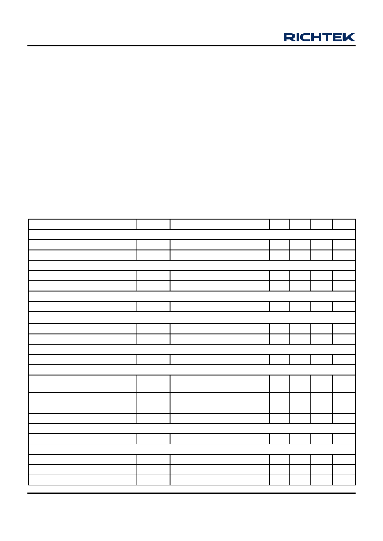
Electrical Characteristics
(VCC = 5V, TA = 25° C, Unless otherwise specified.)
Parameter
Symbol
Test Conditions
VCC Supply Current
Nominal Supply Current
VCC Regulated Voltage
Power-On Reset
ICC
UGATE, LGATE open
VCC
VBOOT = 12V
Rising VCC Threshold
VCC Threshold Hysteresis
Reference
Reference Voltage
VFB
Both PWM and linear regulator
Oscillator
Free Running Frequency
Ramp Amplitude
PWM Error Amplifier
∆ VOSC
DC gain
PWM Controller Gate Driver
Upper Drive Source
Upper Drive Sink
Lower Drive Source
Lower Drive Sink
Linear Regulator
RUGATE
RUGATE
RLGATE
RLGATE
BOOT= 12V
BOOT-VUGATE = 1V
VUGATE = 1V
VCC - VLGATE = 1V,
VLGATE = 1V
DRV Driver Source
Protection
VDRV = 2V
FB Over-Voltage Trip
FB Rising
FB & FBL Under-Voltage Trip
FB & FBL Falling
Soft-Start Interval
Min Typ Max Units
--
3
-- mA
5
6
7
V
3.8 4.1 4.4 V
-- 0.5 --
V
0.784 0.8 0.816 V
250 300 350 kHz
-- 1.75 -- VP-P
32 35 38 dB
-- 7.5 11
Ω
--
5
8
Ω
-- 3.5 6
Ω
--
2
5
Ω
100 --
-- mA
0.9 1
--
V
-- 0.5 0.65 V
-- 2.5 -- ms
www.richtek.com
6
DS9205/A-08 March 2007
Share Link: 