RT9619 データシートの表示(PDF) - Richtek Technology
部品番号
コンポーネント説明
メーカー
RT9619 Datasheet PDF : 11 Pages
| |||
RT9619/A
Application Information
The RT9619/A is designed to drive both high side and low
side N-Channel MOSFET through externally input PWM
control signal. It has power-on protection function which
held UGATE and LGATE low before VCC up across the
rising threshold voltage. After the initialization, the PWM
signal takes the control. The rising PWM signal first forces
the LGATE signal turns low then UGATE signal is allowed
to go high just after a non-overlapping time to avoid shoot-
through current. The falling of PWM signal first forces
UGATE to go low. When UGATE and PHASE signal reach
a predetermined low level, LGATE signal is allowed to turn
high.
The PWM signal is acted as "High" if above the rising
threshold and acted as "Low" if below the falling threshold.
Any signal level enters and remains within the shutdown
window is considered as "tri-state", the output drivers are
disabled and both MOSFET gates are pulled and held
low. If left the PWM signal floating, the pin will be kept
around 2.4V by the internal divider and provide the PWM
controller with a recognizable level.
The RT9619/A typically operates at frequency of 200kHz
to 500kHz. It shall be noted that to place a 1N4148 or
schottky diode between the VCC and BOOT pin as shown
in the typical application circuit for ligher efficiency.
Non-overlap Control
To prevent the overlap of the gate drives during the UGATE
turn low and the LGATE turn high, the non-overlap circuit
monitors the voltages at the PHASE node and high side
gate drive (UGATE-PHASE). When the PWM input signal
goes low, UGATE begins to turn low (after propagation
delay). Before LGATE can turn high, the non-overlap
protection circuit ensures that the monitored voltages have
gone below 1.2V. Once the monitored voltages fall below
1.2V, LGATE begins to turn high. For short pulse condtion,
if the PHASE pin had not gone high after LGATE turns
low, the LGATE has to wait for 200ns before turn high. By
waiting for the voltages of the PHASE pin and high side
gate drive to fall below 1.2V, the non-overlap protection
circuit ensures that UGATE is low before LGATE turns
high.
Also to prevent the overlap of the gate drives during LGATE
turn low and UGATE turn high, the non-overlap circuit
monitors the LGATE voltage. When LGATE go below 1.2V,
UGATE is allowed to go high.
Driving Power MOSFETs
The DC input impedance of the power MOSFET is
extremely high. When Vgs at 12V (or 5V), the gate draws
the current only few nano-amperes. Thus once the gate
has been driven up to "ON" level, the current could be
negligible.
However, the capacitance at the gate to source terminal
should be considered. It requires relatively large currents
to drive the gate up and down 12V (or 5V) rapidly. It also
required to switch drain current on and off with the required
speed. The required gate drive currents are calculated as
follows.
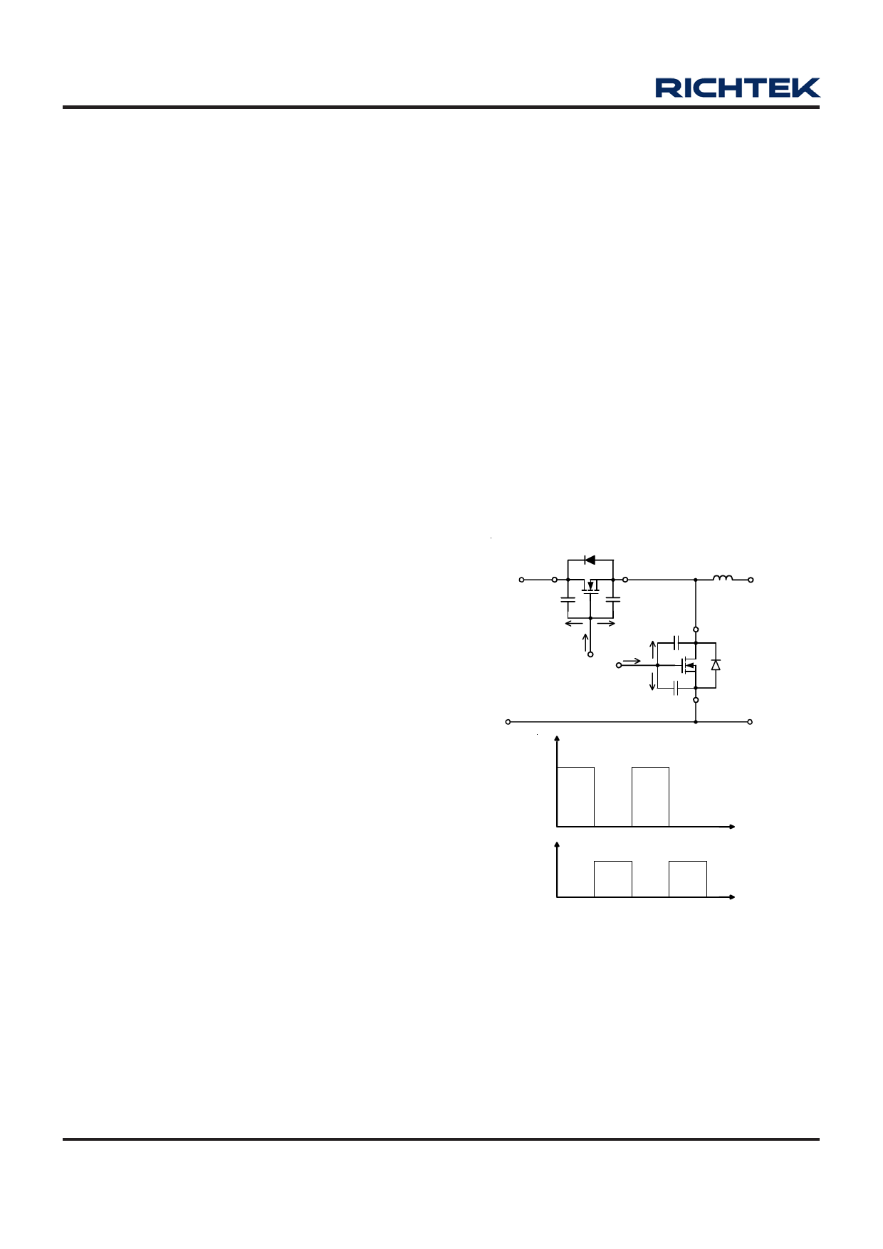
D1
d1
VIN
Cgd1
s1
Cgs1
L
VOUT
Igd1 Igs1
Ig1
g1 g2
Ig2 Igd2
Igs2
Cgd2
d2
D2
Cgs2 s2
Vg1
VPHASE +12V
GND
t
Vg2
12V
t
Figure 1. Equivalent Circuit and Associated Waveforms
In Figure 1, the current Ig1 and Ig2 are required to move the
gate up to 12V. The operation consists of charging Cgd
and Cgs. Cgs1 and Cgs2 are the capacitances from gate to
source of the high side and the low side power MOSFETs,
respectively. In general data sheets, the Cgs is referred as
"Ciss" which is the input capacitance. Cgd1 and Cgd2 are the
capacitances from gate to drain of the high side and the
www.richtek.com
8
DS9619/A-06 April 2011
Share Link: 