RT9501A データシートの表示(PDF) - Richtek Technology
部品番号
コンポーネント説明
メーカー
RT9501A Datasheet PDF : 9 Pages
| |||
RT9501A/B
Preliminary
Absolute Maximum Ratings (Note 1)
z Supply Voltage --------------------------------------------------------------------------------------------------------- −0.3V to 7V
z Storage Temperature Range ---------------------------------------------------------------------------------------- −65°C to 150°C
z Power Dissipation, PD @ TA = 25°C
MSOP-8 ----------------------------------------------------------------------------------------------------------------- 300mW
z Package Thermal Resistance
MSOP-8, θJA ------------------------------------------------------------------------------------------------------------ 80°C/W
z Operation Junction Temperature Range -------------------------------------------------------------------------- −40°C to 125°C
z Junction Temperature ------------------------------------------------------------------------------------------------- 150°C
z ESD Susceptibility (Note 2)
HBM (Human Body Mode) ------------------------------------------------------------------------------------------ 2kV
MM (Machine Mode) -------------------------------------------------------------------------------------------------- 200V
Recommended Operating Conditions (Note 3)
z Supply Input Voltage -------------------------------------------------------------------------------------------------- 4.5V to 7V
z Junction Temperature Range ---------------------------------------------------------------------------------------- −20°C to 70°C
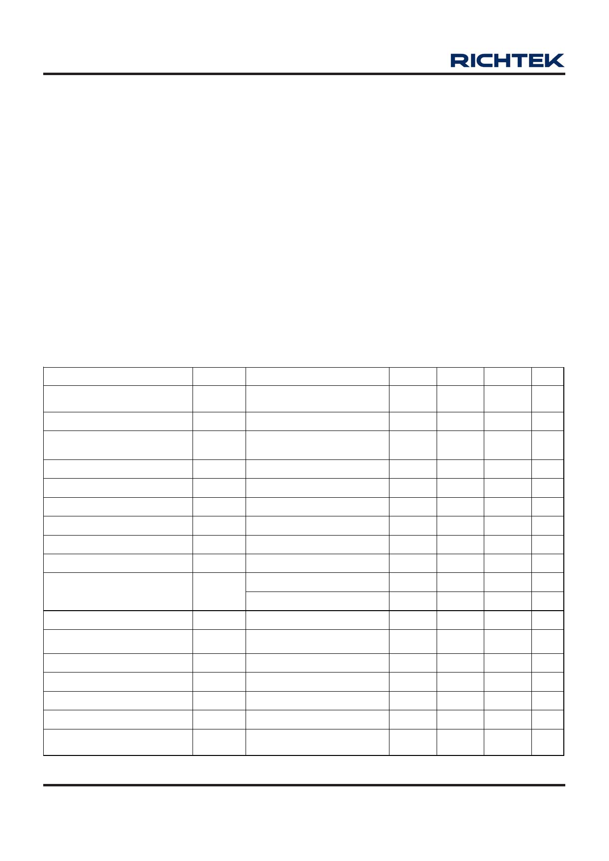
Electrical Characteristics
(TA = 25°C, unless otherwise specification)
Parameter
Symbol
Test Condition
Min
Typ
Max Units
Operating Current
IDD(OPE)
VDD Sleep Current
IDD(SLP)
Input Bias Current @ BATT pin IBATT
Input Bias Current @ CS pin ICS
Input Bias Current @ TS pin ITS
Input Bias Current @ FB/CE pin ICE
Input Low Voltage @ CE pin VCE
Input High Voltage @ CE pin VCE
Feedback Voltage @ FB pin VFB
Output Voltage
VO(REG)
4.5V < VDD < 7V,
--
Excluding external loads
VBATT −VDD ≥ 0.2V
--
VBATT = VO(REG),
--
VBATT − VDD ≥ 0.2V
VCS = 5V, VBATT − VDD ≥ 0.2V
--
VTS = 5V, VBATT − VDD ≥ 0.2V
--
VCE = 5V, VBATT − VDD ≥ 0.2V
--
--
VDD–1.5
2.048
RT9501A
4.059
RT9501B
4.158
1
--
1.5
--
--
--
--
--
2.10
4.10
4.20
2
mA
3
μA
2.5
μA
1
μA
1
μA
1
μA
1.5
V
--
V
2.152 V
4.141 V
4.242 V
Current Regulation Threshold
Charge Terminated Current
Detect Threshold
Lower Temperature Threshold
Upper Temperature Threshold
Precharge Threshold
Precharge Current Regulation
VI(SNS)
V(TERM)
VTS1
VTS2
VO(MIN)
V(PRE)
Recharge Threshold
VO(RCH)
VI(SNS) = VDD – VCS
100
110
121 mV
2
12
22
mV
29.1
30
30.9 %VDD
58.3
60
61.8 %VDD
2.8
2.9
3.0
V
4
14
24
mV
VO(REG) – V O(REG)– VO(REG) – V
140mV 100mV 60mV
To be continued
www.richtek.com
4
DS9501A/B-07 March 2007
Share Link: 