S4242 データシートの表示(PDF) - Summit Microelectronics
部品番号
コンポーネント説明
メーカー
S4242 Datasheet PDF : 16 Pages
| |||
S4242/S42WD42/S4261/S42WD61
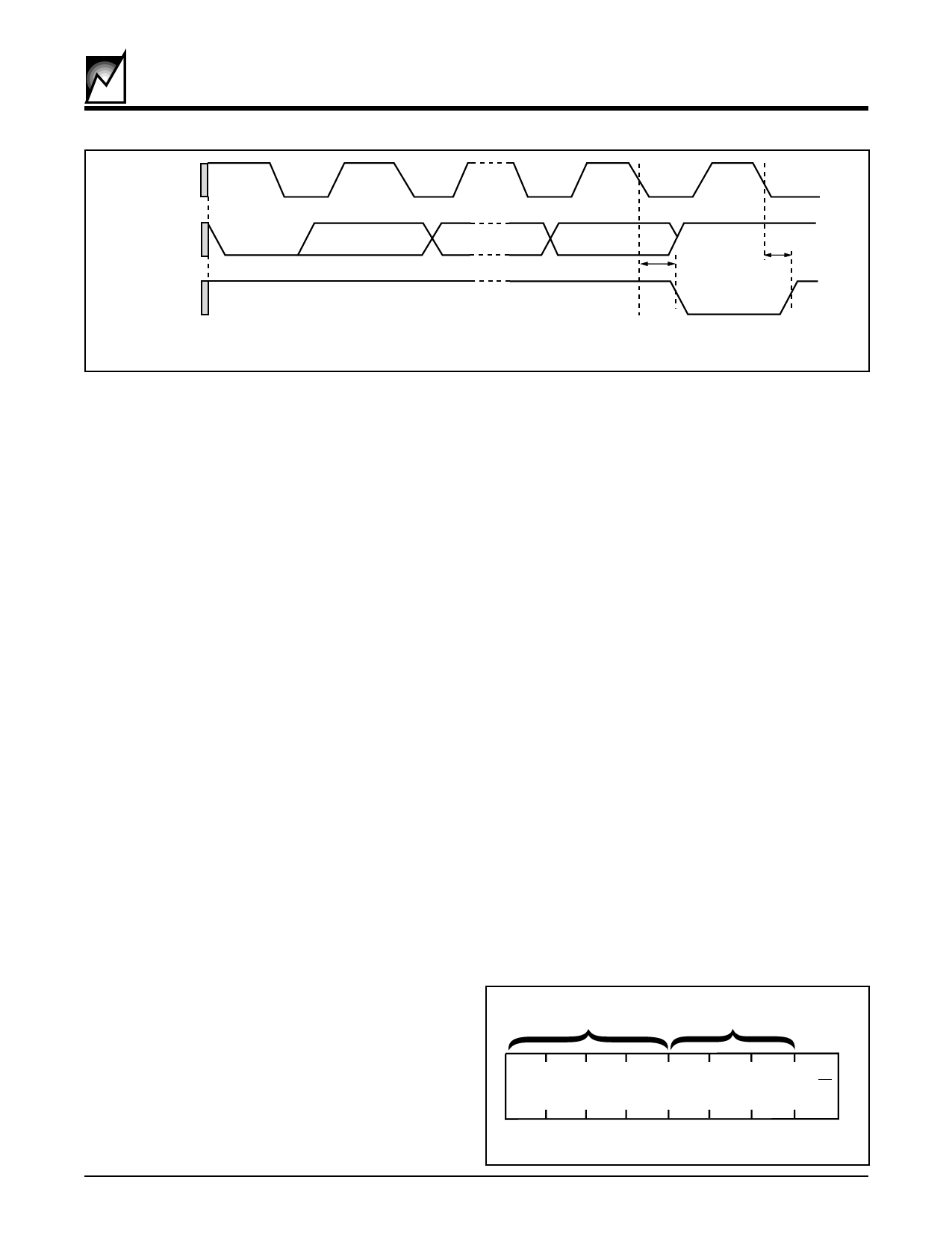
SCL from
Master
1
Start
Data Output Condition
from
Transmitter
8
9
tAA
Data Output
from
Receiver
tAA ACKnowledge
FIGURE 8. ACKNOWLEDGE RESPONSE FROM RECEIVER
2025 ILL8.0
CHARACTERISTICS OF THE I2C BUS
General Description
The I2C bus was designed for two-way, two-line serial
communication between different integrated circuits. The
two lines are: a serial data line (SDA), and a serial clock
line (SCL). The SDA line must be connected to a positive
supply by a pull-up resistor, located somewhere on the
bus (See Figure 6). Data transfer between devices may
be initiated with a START condition only when SCL and
SDA are HIGH (bus is not busy).
Input Data Protocol
One data bit is transferred during each clock pulse. The
data on the SDA line must remain stable during clock
HIGH time, because changes on the data line while SCL
is HIGH will be interpreted as start or stop condition, refer
to Figure 2.
START and STOP Conditions
When both the data and clock lines are HIGH, the bus is
said to be not busy. A HIGH-to-LOW transition on the data
line, while the clock is HIGH, is defined as the “START”
condition. A LOW-to-HIGH transition on the data line,
while the clock is HIGH, is defined as the “STOP” condi-
tion (See Figure 2).
DEVICE OPERATION
The S42xxx is a 16K-bit serial E2PROM. The device
supports the I2C bidirectional data transmission protocol.
The protocol defines any device that sends data onto the
bus as a “transmitter” and any device which receives data
as a “receiver.” The device controlling data transmission
is called the “master” and the controlled device is called
the “slave.” In all cases, the S42xxx will be a “slave”
device, since it never initiates any data transfers.
will pull the SDA line LOW to ACKnowledge that it received
the eight bits of data (See Figure 8).
The S42xxx will respond with an ACKnowledge after
recognition of a START condition and its slave address
byte. If both the device and a write operation are selected,
the S42xxx will respond with an ACKnowledge after the
receipt of each subsequent 8-bit word.
In the READ mode, the S42xxx transmits eight bits of
data, then releases the SDA line, and monitors the line for
an ACKnowledge signal. If an ACKnowledge is detected,
and no STOP condition is generated by the master, the
S42xxx will continue to transmit data. If an ACKnowledge
is not detected, the S42xxx will terminate further data
transmissions and awaits a STOP condition before return-
ing to the standby power mode.
Device Addressing
Following a start condition the master must output the
address of the slave it is accessing. The most significant
four bits of the slave address are the device type identifier
(see figure 7). For the S42xxx this is fixed as 1010[B].
Word Address
The next three bits of the slave address are an extension
of the array’s address and are concatenated with the eight
bits of address in the word address field, providing direct
access to the 2,048 x8 array of the S4261 and S42WD61.
A10 and A9 are “Don’t Care” on S4242 and S42WD42.
Read/Write Bit
The last bit of the data stream defines the operation to be
performed. When set to “1,” a read operation is selected;
when set to “0,” a write operation is selected.
DEVICE
IDENTIFIER
HIGH ORDER
WORD ADDRESS
Acknowledge (ACK)
Acknowledge is a software convention used to indicate
successful data transfers. The transmitting device, either
the master or the slave, will release the bus after transmit-
ting eight bits. During the ninth clock cycle, the receiver
10
*
*
1 0 A10 A9 A8 R/W
*S4261/S42WD61 only
2025 ILL9.1
FIGURE 9. SLAVE ADDRESS BYTE
2025 6.0 4/17/00
8
Share Link: 