SA702 データシートの表示(PDF) - Philips Electronics
部品番号
コンポーネント説明
メーカー
SA702 Datasheet PDF : 7 Pages
| |||
Philips Semiconductors RF Communications Products
Divide by: 64/65/72 triple modulus low power
ECL prescaler
Product specification
SA702
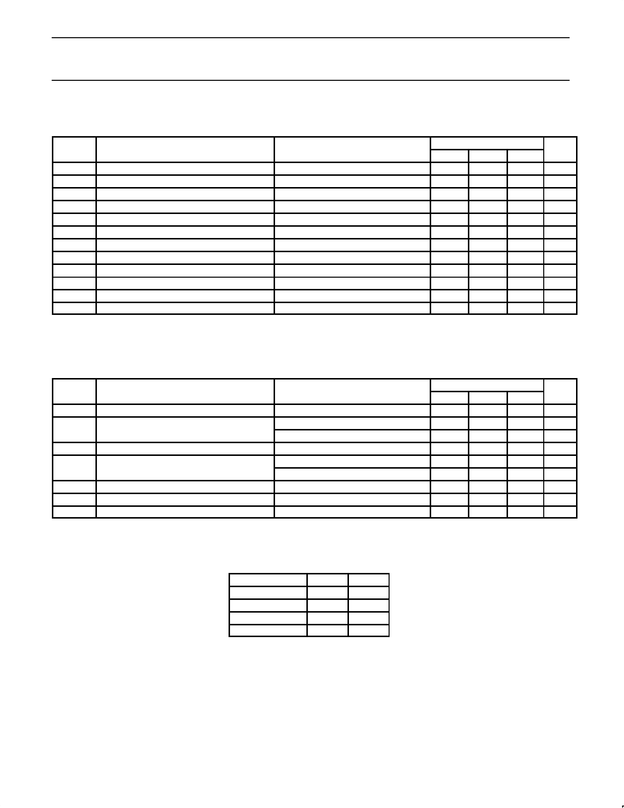
DC ELECTRICAL CHARACTERISTICS
The following DC specifications are valid for TA = 25°C and VCC = 3.0V; unless otherwise stated. Test circuit Figure 1.
SYMBOL
PARAMETER
TEST CONDITIONS
LIMITS
MIN
TYP
VCC Power supply voltage range
ICC
Supply current
VOH Output high level
VOL Output low level
VIH MC1 input high threshold
VIL
MC1 input low threshold
VIH MC2 input high threshold
VIL
MC2 input low threshold
IIH
MC1 input high current
IIL
MC1 input low current
IIH
MC2 input high current
IIL
MC2 input low current
fIN = 1GHz, input level = 0dBm
No load
IOUT = 1.2mA
VMC1 = VCC = 6V
VMC1 = 0V, VCC = 6V
VMC2 = VCC = 6V
VMC2 = 0V, VCC = 6V
2.7
VCC-1.4
2.0
–0.3
2.0
–0.3
–100
–100
4.5
VCC-2.6
0.1
–30
0.1
–30
MAX
6.0
VCC
0.8
VCC
0.8
50
50
UNITS
V
mA
V
V
V
V
V
V
µA
µA
µA
µA
AC ELECTRICAL CHARACTERISTICS
These AC specifications are valid for fIN = 1GHz, input level = 0dBm, VCC = 3.0V and TA = 25°C; unless otherwise stated. Test circuit Fig. 1.
SYMBOL
PARAMETER
TEST CONDITIONS
LIMITS
UNITS
VIN
Input signal amplitude1
fIN
Input signal frequency
1000pF input coupling
Direct coupled input2
1000pF input coupling
MIN
0.05
0
TYP MAX
2.0
VP-P
1.1 GHz
1.1 GHz
RID Differential input resistance
VO
Output voltage
tS
Modulus set-up time1
tH
Modulus hold time1
tPD
Propagation time
DC measurement
VCC = 5.0V
VCC = 3.0V
5
kΩ
1.6
VP-P
1.2
VP-P
5
ns
0
ns
10
ns
NOTES:
1. Maximum limit is not tested, however, it is guaranteed by design and characterization.
2. For fIN < 50MHz, minimum input slew rate of 32V/µs is required.
DESCRIPTION OF OPERATION
The SA702 comprises a frequency divider
circuit implemented using a divide by 4 or 5
synchronous prescaler followed by a 5 stage
synchronous counter, see BLOCK
DIAGRAM. The normal operating mode is for
MC1 (Modulus Control) to be set high and
MC2 input to be set low in which case the
circuit comprises a divide by 64. For divide
by 65 the MC1 singal is forced low, causing
the prescaler circuit to switch into divide by 5
operation for the last cycle of the
synchronous counter. For divide by 72, MC2
is set high configuring the prescaler to divide
by 4 and the counter to divide by 18. A truth
table for the modulus values is given below:
Table 1.
Modulus
64
65
72
72
MC1
1
0
0
1
MC2
0
0
1
1
For minimization of propagation delay effects,
the second divider circuit is synchronous to
the divide by 4/5 stage output.
The prescaler input is positive edge sensitive,
and the output at the final count is a falling
edge with propagation delay tPD relative to
the input. The rising edge of the output
occurs at the count 32 with delay tPD.
The MC1 and MC2 inputs are TTL
compatible threshold inputs operating at a
reduced input current. CMOS and low
voltage interface capability are allowed.
The prescaler input is differential and ECL
compatible. The output is differential ECL
compatible.
June 17, 1993
4
Share Link: 