SC1403(2002) データシートの表示(PDF) - Semtech Corporation
部品番号
コンポーネント説明
メーカー
SC1403 Datasheet PDF : 30 Pages
| |||
SC1403
POWER MANAGEMENT
PRELIMINARY
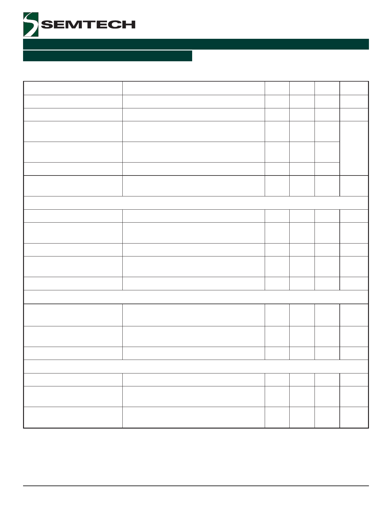
Electrical Characteristics (Cont.)
Unless otherwise noted: V+ = 15V, both PWMs on, SYNC = 0V, VL load = 0mA, REF load = 0mA, PSAVE# = 0V, TA =-40 to 85°C. Typical values are at
TA = +25°C. Circuit = Typical Application Circuit
Parameter
Conditions
Min Typ Max Units
REF Sink Current
REF Fault Lockout Voltage
V+ Operating Supply Current
V+ Standby Supply Current
V+ Shutdown Supply Current
Quiescent Power Consumption
FAULT DETECTION
10
µA
Falling edge
1.8
2.2
V
VL switched over to VOUT5, both SMPS on,
ILoad3 = 0A, ILoad5 = 0A
10
50
µA
V+ = 6V to 30V, SMPS off,
180
includes current into SHDN#
V+ = 6V to 30V, SHDN# = 0V
4
10
SMPS enabled, FB3 = FB5 = 0V,
No Load on SMPS
6.0
mW
Overvoltage Trip Threshold
With respect to unloaded output voltage
7
10
15
%
Overvoltage-Fault
Propagation Delay
Output driven 2% above overvoltage trip VTH
1.5
µs
Output Undervoltage Threshold
With respect to unloaded output voltage
65
75
85
%
Output Undervoltage Lockout
Time
From each SMPS enabled, with respect to f OSC 5000 6144 7000 clks
Thermal Shutdown Threshold
Typical hysteresis = +10°C
150
°C
RESET#
RESET# Trip Threshold
With respect to unloaded output voltage,
-13 -10
-7
%
falling edge; typical hysteresis = 1%
RESET# Propagation Delay
RESET# Delay Time
INPUTS AND OUTPUTS
Falling edge, output driven 2% below
RESET# trip threshold
With respect to fOSC
1.5
µs
27,000 32,000 37,000 clks
Feedback Input Leakage Current
FB3, FB5 = 2.6V
Logic Input Low Voltage
ON3, PSAVE#, ON5, SHDN#, SYNC
(SEQ = 0V or VL)
Logic Input High Voltage
ON3, PSAVE#, ON5, SHDN#, SYNC
2.4
(SEQ = 0V or VL)
+1
µA
0.6
V
V
2002 Semtech Corp.
4
www.semtech.com
Share Link: 