SERC816 データシートの表示(PDF) - STMicroelectronics
部品番号
コンポーネント説明
メーカー
SERC816 Datasheet PDF : 23 Pages
| |||
SERCON816
4 CONTROL REGISTERS AND RAM DATA STRUCTURES
4.1 Control Register Addresses
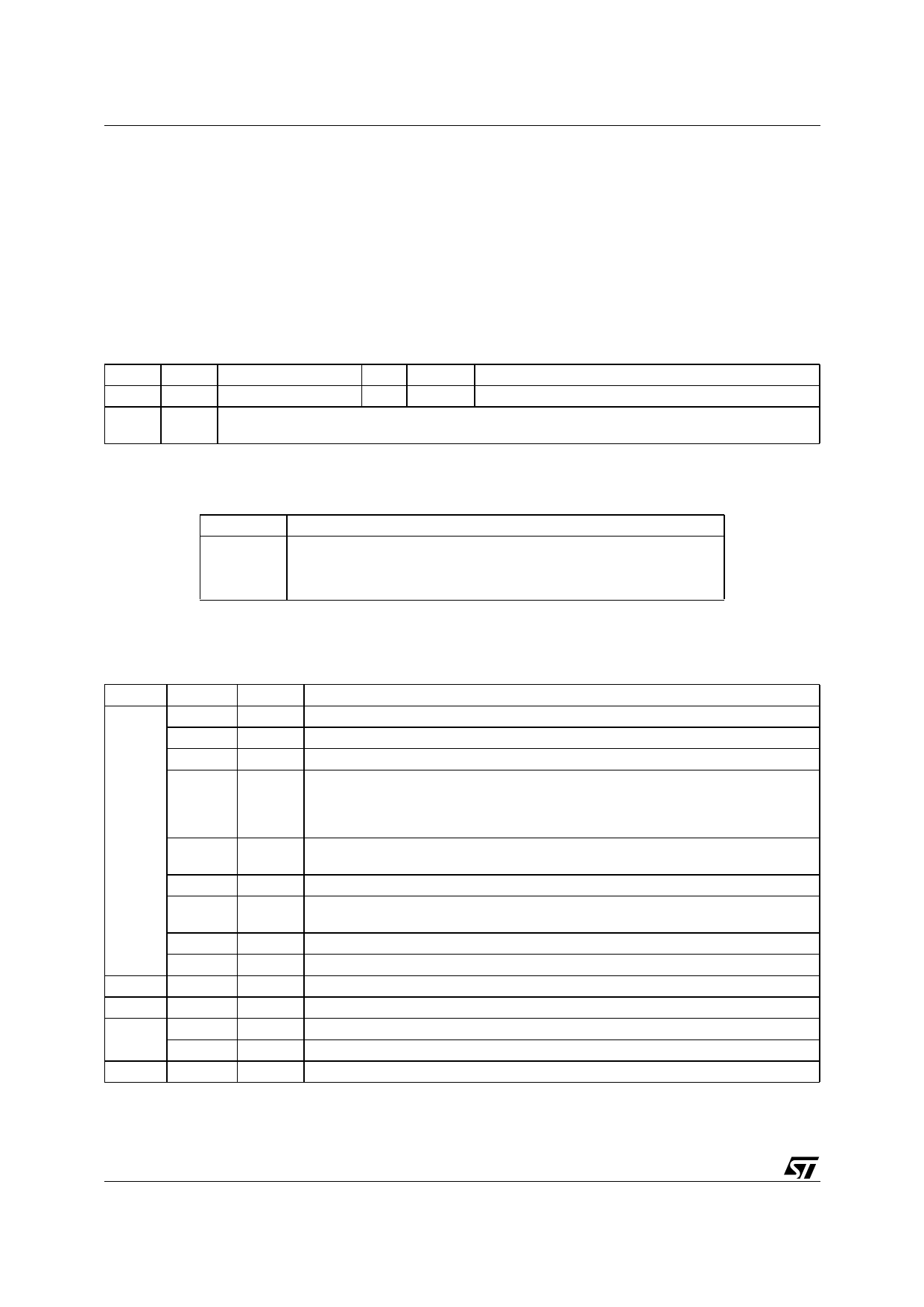
The following table is an overview of the control registers. The address is the word address which is input
by A6-1. To calculate the byte address, the value has to be multiplied by two. All control registers can be
written to and read (R/W), with the exception of the control bits that initiate an action (W).
The status registers can only be read (R). When control registers which contain bits that are not used or
can only be read, are written to, these bits can be set to 0 or 1; they are not evaluated internally. If control
registers are read with bits that are not used, these bits are set to 0.
A6-1
00H
01H
- 2AH
Bits
0-15
0-15
Name
R/W Value
Function
VERSION
R 0010H Circuit code (0010H)
Please refer to SERCON816 Reference Guide for a detailed description of the control registers.
4.2 Data Structures within the RAM
In this RAM the first eleven words have a fixed meaning.
A10-1
Contents
0-1
COMPT0-1: Start of transmission blocks 0-1
2-9
SCPT0-7: Address service containers 0-7
10
NMSTERR: Error counter MST
The rest of the RAM can be divided into data structures as required.
4.2.1 Telegram Headers
A telegram header for receive telegram contains the following five control words:
Index
0
1
2
3
4
Bit
0-7
8
9
10
11
12
13
14
15
0-15
0-15
0-10
9-15
0-15
Name
ADR
DMA
DBUF
VAL
ACHK
TCHK
RERR
0
0
TRT
TLEN
PT
NERR
Function
Telegram address
Data storage in the internal RAM (DMA = 0) or DMA transfer (DMA = 1)
Data in the RAM: single buffer (DBUF = 0) or double buffer (DBUF = 1)
For single buffering (DMA = 0, DBUF = 0) or DMA transfer (DMA = 1): telegram data
is invalid (VAL = 0) or valid (VAL = 1); for double buffering (DMA = 0, DBUF = 1): data
in buffer 0 (VAL = 0) or buffer 1 (VAL = 1) is valid. Modified by controller at beginning
and end of receive telegrams.
Telegrams are received if the address is valid (ACHK = 1) or independent on the
received address (ACHK = 0). The received address is stored at ADR.
The time of receiving is checked (TCHK = 1) or not checked (TCHK = 0).
The last telegram was free of error (RERR = 0) or errored or not received (RERR =
1).
Marker bit for telegram header of receive telegram.
Marker bit for telegram header.
Time for the start of telegram in µs after end of MST.
Length of telegram in data words (not including address).
Word address within the RAM of the next telegram header or the end marker.
(Not used)
Error counter
16/23
Share Link: 