SERC816 データシートの表示(PDF) - STMicroelectronics
部品番号
コンポーネント説明
メーカー
SERC816 Datasheet PDF : 23 Pages
| |||
SERCON816
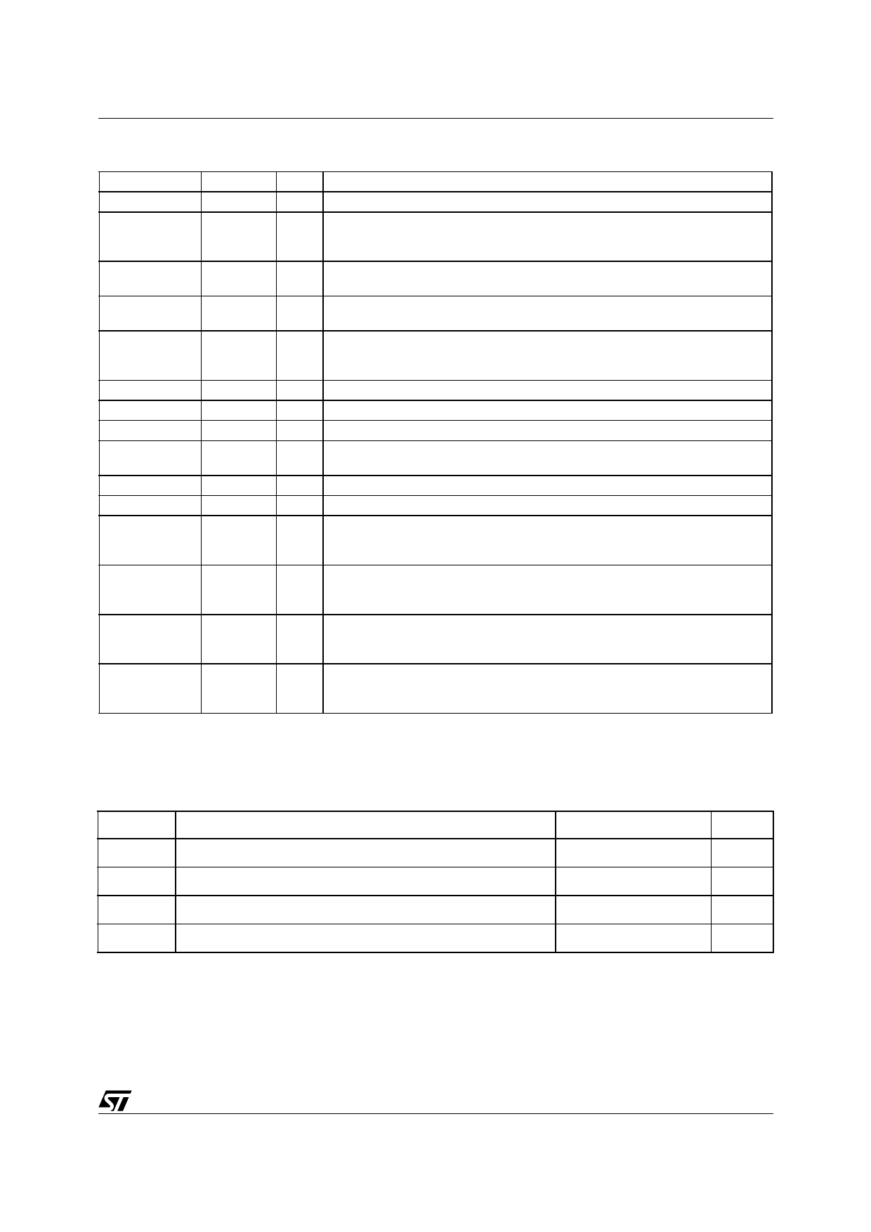
Table 1. SERCON816 I/O Port Function Summary (continued)
Signal(s)
WDOGN
L_ERRN
CYC_CLK
CON_CLK
DIV_CLK
SCLK
SCLKO2
SCLKO4
MCLK
RSTN
TEST
OUTZ
NDTRO
VSS
VDD
Pin(s)
IO
Function
24
O Watchdog output (active low)
32
O Line error, active low: goes low when signal distortion is too high or when the
receive signal is missing. The operating mode is programmed by the
processor.
34
I SERCOS interface cycle clock: CYC_CLK synchronizes the communication
cycles. The polarity is programmable.
35
O Control clock: becomes active within a communication cycle. Time, polarity
and width are programmable.
36
O Divided control clock: becomes active several times within a communication
cycle or once in several communication cycles. Number of pulses, start time,
repetition rate and polarity are programmable, the pulse width is 1 µs.
2
I Serial clock for clock regeneration: the maximum frequency is 64 MHz.
6
O Clock output: outputs the SCLK clock divided by 2 or 1.
5
O Clock output: outputs the SCLK clock divided by 4 or 2.
4
I Master clock for telegram processing and timing control, frequency 12 to 64
MHz.
10
I Reset, active low. Must be zero for at least 50 ns after power on.
7
I Test, active high. Has to be tied to VSS.
11
I Puts outputs into high impedance state, active high: OUTZ is 1 puts all pins
into a high impedance state. The clocks are turned off and the circuit is reset.
For the in-circuit test and for turning on the power-down mode.
9
O NAND tree output. For the test at the semiconductor manufacturers and for
the connection test after board production. NDTRO is not set to a high
impedance state.
3,15,23,33
,42,50,60,
70,81,91
Ground pins:
1,8,19,27,
37,55,65,
76,86
Power supply +5 V ± 5%.
3 ELECTRICAL (DC AND AC) CHARACTERISTICS
3.1 Absolute Maximum Ratings
Symbol
Parameter
VDD
Supply voltage
VI
Input voltage
VO
Output voltage
TSTG Storage temperature
Value
-0.5 to 6.5
-0.5 to VDD + 0.5
-0.5 to VDD + 0.5
-55 to +150
Unit
V
V
V
°C
7/23
Share Link: 