SIP12202DM-T1-E3 データシートの表示(PDF) - Vishay Semiconductors
部品番号
コンポーネント説明
メーカー
SIP12202DM-T1-E3 Datasheet PDF : 10 Pages
| |||
SiP12202
Vishay Siliconix
New Product
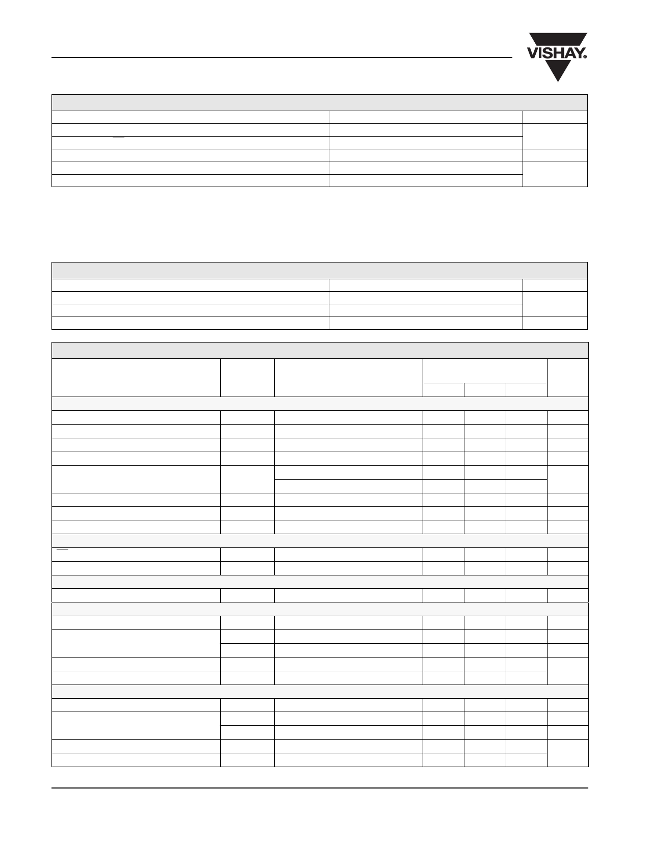
ABSOLUTE MAXIMUM RATINGS
Parameter
VIN, LX to GND
FB, PG, Comp/SD to GND
Power Dissipationa, b
Maximum Junction Temperature
Storage Temperature
Limit
Unit
6
V
- 0.3 to 6
560
mW
125
°C
- 55 to + 150
Notes
a. Device mounted with all leads soldered or welded to PC board
b. Derate 14 mW/°C above + 85 °C
Stresses beyond those listed under "Absolute Maximum Ratings" may cause permanent damage to the device. These are stress ratings only,
and functional operation of the device at these or any other conditions beyond those indicated in the operational sections of the specifications is
not implied. Exposure to absolute maximum rating/conditions for extended periods may affect device reliability.
RECOMMENDED OPERATING RANGE
Parameter
Input Voltage Range
Output Voltage Adjustment Range
Operating Temperature Range
Limit
Unit
2.7 to 5.5
V
0.6 to 5.5
- 40 to + 85
°C
SPECIFICATIONS
Parameter
Controller
Input Voltage
Quiescent Current
Switching Oscillator Frequency
Oscillator Ramp Amplitude
Feedback Voltage
FB input Bias Current
Transconductance
Soft Start
Inputs and Outputs
SD Input Voltage
Shutdown Current
MOSFET Drivers
Break-before-make-time
Highside Driver
Output Voltage
On resistance
Rise time - PFET Turn On
Fall time - PFET Turn Off
Lowside Driver
Output Voltage
On resistance
Rise time - NFET Turn On
Fall time - NFET Turn Off
Limits
Symbol
Test Condition Unless Specified
VIN = 5.0
-40 to 85°C
Mina
Typb
Maxa
Unit
VIN
fOSC
∆VOSC
VFB
IFB
GM
Non Switching
TA = 25 °C
2.7
400
0.591
0.585
0.6
500
1
0.600
2
4
5.5
1
600
0.609
0.615
100
V
mA
kHz
V
V
nA
mA/V
ms
VIL
IIL
tBBM
VDH
RDSHH
RDSHL
trH
tfH
VIN = 4.5 V
VIN = 4.5 V
VIN = 5 V, CL = 2.7 nF
VIN = 5 V, CL = 2.7 nF
0.15
V
30
60
µA
30
ns
4.5
V
1.3
1.9
Ω
2.8
4.4
Ω
64
ns
8
VDL
RDSLH
RDSLL
trL
tfL
VIN = 4.5 V
VIN = 4.5 V
VIN = 5 V, CL = 2.7 nF
VIN = 5 V, CL = 2.7 nF
4.5
V
5.5
8.2
Ω
0.85
1.4
Ω
83
ns
6.6
www.vishay.com
2
Document Number: 73542
S-52083–Rev. A, 10-Oct-05
Share Link: 