SIP12506 データシートの表示(PDF) - Vishay Semiconductors
部品番号
コンポーネント説明
メーカー
SIP12506 Datasheet PDF : 13 Pages
| |||
SiP12506
Vishay Siliconix
Product is End of Life 3/2014
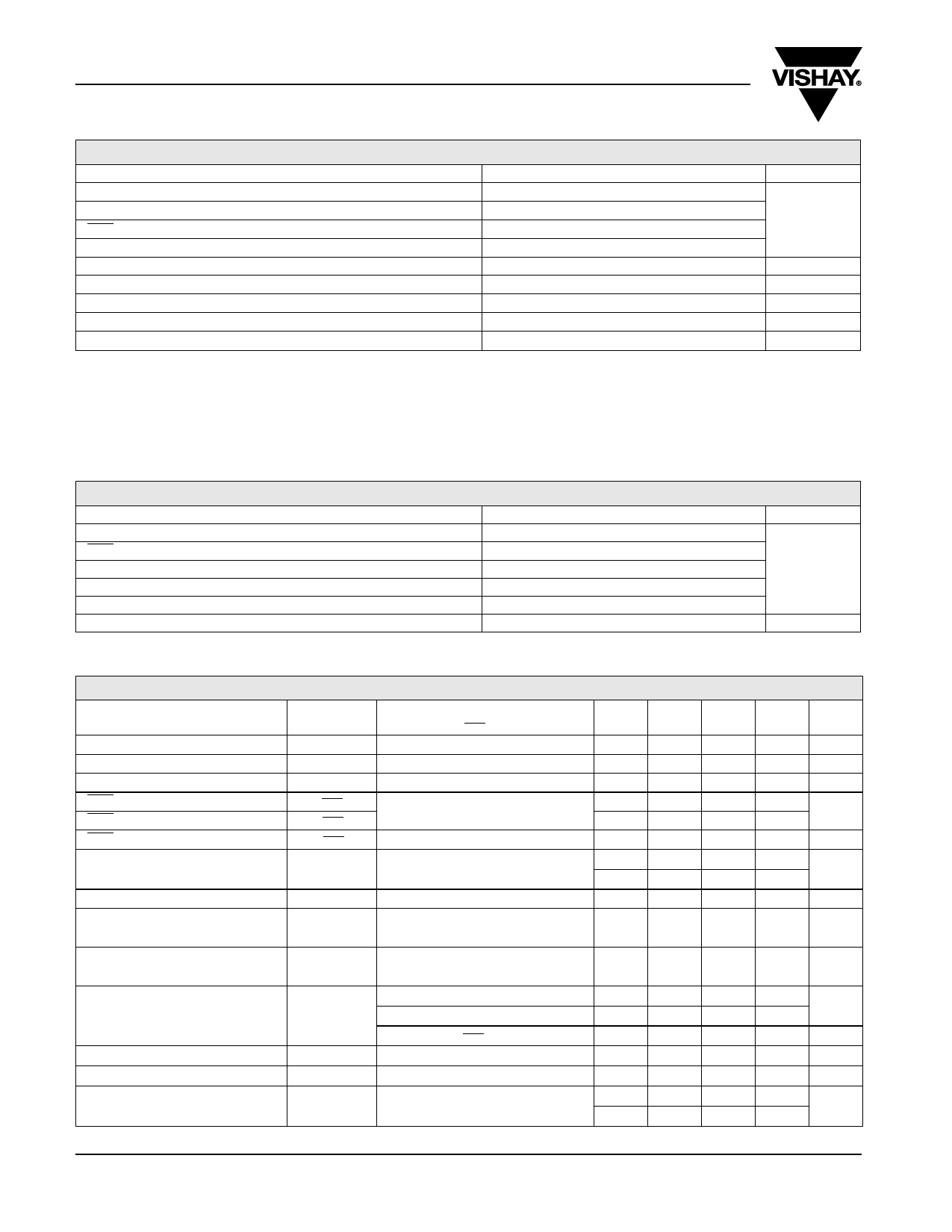
ABSOLUTE MAXIMUM RATINGS
Parameter
Limit
Unit
Voltages Referenced Input Voltage VIN to GND
VOUT, LX Voltages
SHD Voltage
FB Voltage
ESD (Human Body Model)a
- 0.3 to 12
- 0.3 to 28
V
- 0.3 to 12
- 0.3 to 12
2
kV
Operating Junction Temperature
125
°C
Storage Temperature
Power Dissipation (TA = 70 °C)b
Thermal Resistancec
- 55 to + 150
1100
50
°C
mW
°C/W
Notes:
a. The human body model is a 100 pF capacitor discharged through a 1.5 kΩ resistor into each pin.
b. Derate 20 mW/°C above 70 °C.
c. Devise mounted with all leads soldered or welded to PC board.
Stresses beyond those listed under "Absolute Maximum Ratings" may cause permanent damage to the device. These are stress ratings only, and functional operation
of the device at these or any other conditions beyond those indicated in the operational sections of the specifications is not implied. Exposure to absolute maximum
rating/conditions for extended periods may affect device reliability.
RECOMMENDED OPERATING RANGE
Parameter
Voltages Referenced Input Voltage Range (VIN) to GND
SHD
VOUT
LX
FB
Operating Temperature Range
Limit
Unit
2.6 to 9
0 to VIN
VIN to 18
V
0 to 18.5
0 to 2
- 40 to 85
°C
SPECIFICATIONS
Parameter
Input Voltage
Switch Current Limit
Switch on Resistance
SHD Input High Level
SHD Input Low Level
SHD Input Leakage Current
Symbol
VIN
ILIMIT
RDS(on)
VSHDH
VSHDL
ISHD
Test Conditions Unless Specified
VIN = 5.0 V, VSHD = 2 V, TA = 25 °C
ISW = 200 mA
VIN = 2.6 to 9 V
Feedback Voltage
VFB
Feedback Bias Current
Feedback Voltage Line Regulation
Feedback Voltage Load Regulation
IFB
Δ VFB/
(VFB x Δ VIN)
Δ VFB/
(VFB x Δ VOUT)
Quiescent Current
Switching Frequency
Maximum Duty Cycle
I VIN
FSW
DMAX
VIN = 2.6 V to 9 V
VOUT = 10 V
VFB = 0 V (Switching)
VFB = 1.5 V (Not Switching)
VSHD = 0 V
Switch Leakage
ILEAK
Not Switching, VLX = 5 V
Temp
FULL
FULL
FULL
FULL
FULL
25 °C
FULL
FULL
FULL
FULL
FULL
FULL
FULL
25 °C
FULL
Mina
2.6
1.1
1.5
0.198
0.188
0.75
86
Typb
1.6
0.4
0.208
60
0.2
0.15
2.1
0.35
1
91
Maxa
9
2.2
0.65
0.5
1
0.218
0.224
3.0
0.5
1
1.25
1
5
Unit
V
A
Ω
V
µA
V
nA
%/V
%/A
mA
µA
MHz
%
µA
www.vishay.com
2
Document Number: 73861
S-70547–Rev. D, 26-Mar-07
Share Link: 