SIP12506DMP-TI-E3 データシートの表示(PDF) - Vishay Semiconductors
部品番号
コンポーネント説明
メーカー
SIP12506DMP-TI-E3 Datasheet PDF : 13 Pages
| |||
Product is End of Life 3/2014
SiP12506
Vishay Siliconix
SPECIFICATIONS
Thermal Shutdown
Thermal Shutdown Hysteresis
Under Voltage Lockout
UVLO Hysteresis
OVLO
OVLO Hysteresis
OUT Bias Current
TSHD
THYST
TUVLO
TUVLOHYST
TOVLO
TOVLOHSYST
IVOUT
VIN Rising
VOUT Rising
VOUT = 5 V
160
°C
25
FULL 2.25
2.4
2.55
0.1
V
FULL 18
20
22.5
1
3.2
µA
Notes:
a. Limits are guaranteed by testing.
b. Typical values are derived from the mean value of a large quantity of samples tested during characterization and represent the most likely
expected value of the parameter at room temperature.
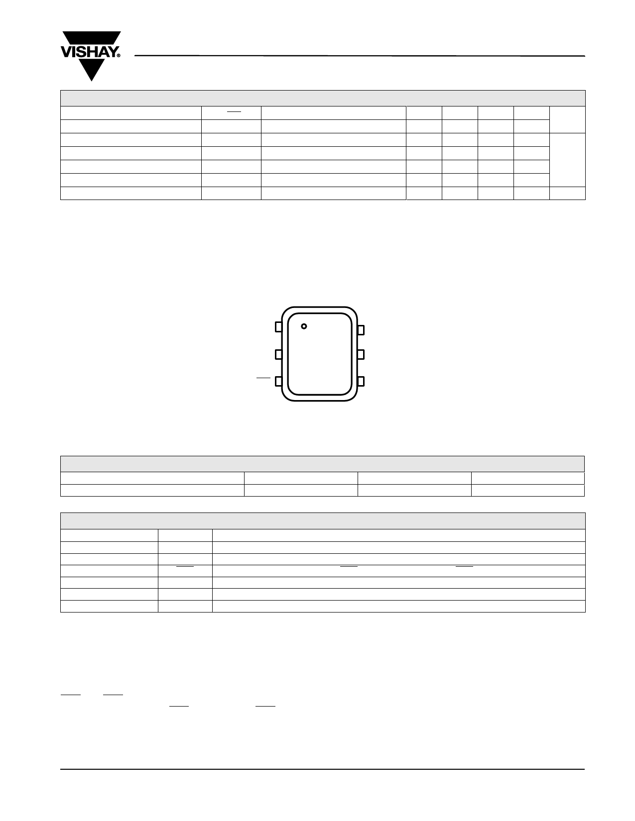
PIN CONFIGURATION
6 Lead MLP33 Package
LX
1
VIN
2
SHD
3
6
GND
5
VOUT
4
FB
Top View
Figure 3.
ORDERING INFORMATION
Part Number
SiP12506DMP-TI-E3
Marking
2506
Temperature Range
- 40 °C to 85 °C
Package
MLP33-6
PIN DESCRIPTION
Pin Number
Name
1
LX
2
VIN
3
SHD
4
FB
5
VOUT
6
GND
Function
Drain Pin of the Internal Switch.
Input Power Pin.
Logic Controlled Shutdown Input. SHD = high: Normal operation. SHD = low: Shutdown.
Voltage Feedback Pin.
Output Voltage Pin.
Signal and Power Ground.
DETAILED PIN DESCRIPTION
LX: Drain of the Internal 26 V NMOS. Connect inductor/
diode to LX. Minimize trace area at this pin to keep electro-
magnetic interference down to a minimum.
VIN: the analog and power input of the controller IC. A bypass
capacitor is required on this pin.
SHD: the SHD pin provides shutdown control. To allow for
normal operation, connect SHD to VIN. Connect SHD to GND
to disable the device.
FB: The inverting input of the voltage error amplifier. This is
internally compared against a voltage of 0.208 V appearing
on the voltage error amplifier's non-inverting input. External
resistors are connected to this pin to set the regulated output
voltage.
VOUT: Output voltage sense for over voltage protection and
slop compensation.
GND: This pin acts as both the analog ground and the power
ground for this part.
Document Number: 73861
S-70547–Rev. D, 26-Mar-07
www.vishay.com
3
Share Link: 