SIP12506DMP-TI-E3 データシートの表示(PDF) - Vishay Semiconductors
部品番号
コンポーネント説明
メーカー
SIP12506DMP-TI-E3 Datasheet PDF : 13 Pages
| |||
SiP12506
Vishay Siliconix
Product is End of Life 3/2014
FUNCTIONAL BLOCK DIAGRAM
V OUT
V IN
LX
FB
SHD
0.208 V
Reference
-
Vc
Gm
+ Cc1
Rc
Softstart
Ramp
Generator
Cc2
Shutdown
Control
Oscillator
Thermal
Shutdown
-
PWM
∑+
R FF
RQ
RS
Driver
Current Limit
Comparator
Current Sense
+
-
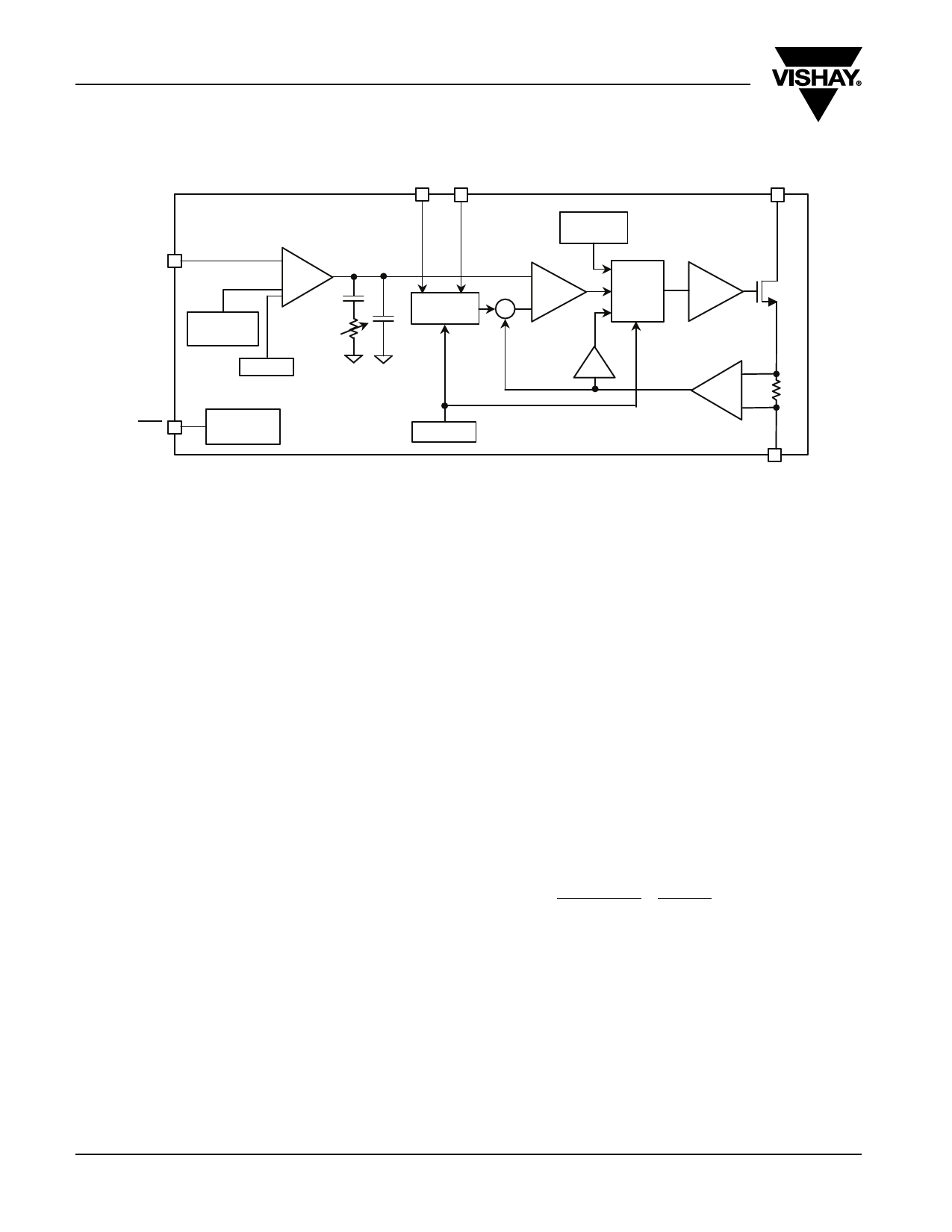
Figure 4. Internal Block Diagram
GND
DETAILED OPERATION DESCRIPTION:
The SiP12506 is a current mode, internally compensated,
step-up switching converter that operates at a fixed fre-
quency of 1 MHz. The current mode topology allows for fast
transient response over a wide input range and provides a
real-time, cycle-by-cycle current limiting function. The opera-
tion of the converter can be described through the interaction
of two separate internal loops: the current sense loop and
voltage sense loop.
Within the current sense loop, the switch FET current is mon-
itored by sensing the voltage across an internal current
sense resistor which is fed to the inputs of both the current
limit amplifier and the pulse width modulation (PWM) com-
parator.
At the beginning of each switch cycle, the oscillator sets the
S-R latch thereby turning on the FET. As current through the
switch increases, so does the voltage drop across the sense
resistor. This voltage is summed with the ramp coming from
the ramp generator and applied to the input of the PWM com-
parator. When this ramping voltage exceeds Vc (the output
of the Gm amplifier), the latch changes state and turns off the
FET. The slope of the ramp generator is proportional to volt-
ages on the VIN and VOUT pins, therefore, any sudden
changes in input or output voltage can be corrected and
accommodated for on a cycle-by-cycle basis. If the FET cur-
rent surpasses the current limit threshold, the current limit
comparator will unconditionally turn off the internal power
switch. At the beginning of the next oscillator cycle, the
switch is allowed to turn on again.
The voltage feedback loop works by monitoring the LED
drive current through a resistor divider on FB and comparing
that voltage with an internal reference voltage (Vref). If the
LED current falls below the set current, the voltage on the
feedback pin will drop slightly below Vref causing Vc to
increase. This will keep the PWM comparator's output high
for a greater portion of an oscillator cycle, thus ensuring that
the FET will stay on longer. This, in turn, will allow more cur-
www.vishay.com
6
rent to be delivered to the load. Following similar logic,
should the LED current become higher than the set current,
FB voltage will increase above Vref, the converter will
decrease its duty cycle, which will lessen the energy deliv-
ered to the load at each cycle, and thereby, reduce LED cur-
rent and maintain desired brightness.
In essence, by modifying the on time of the switch, the PWM
comparator continually sets the correct maximum current
through the FET to regulate the LED current to a desired
value.
POWER DISSIPATION CONSIDERATIONS:
An important consideration when designing power convert-
ers is the maximum allowable power dissipation of a part.
The maximum power dissipation in any application is
dependant on the maximum junction temperature,
TJ(MAX) = 125 °C, the junction-to-ambient thermal resistance
for the MLP33-6 package, ΘJ-A = 50 °C/W, and the ambient
temperature, TA, which may be formulaically expressed as:
P(MAX) = TJ (MAX) - TA = 125 - TA
θ J-A
50
It then follows that, assuming an ambient temperature of
70 °C, the maximum power dissipation will be limited to about
1.1 watts.
In the event that the power dissipation exceeds the value
specified above and the die temperature reaches 160 °C, the
internal thermal protection circuitry will ensure safe operation
by turning off the internal FET, thereby maintaining junction
temperature at a safe level. In this state, only the system
monitor circuitry will be active. Once the temperature of the
chip drops below 135 °C, the chip re-enters soft-start mode
and resumes normal operation.
Document Number: 73861
S-70547–Rev. D, 26-Mar-07
Share Link: 