SIP12506DMP-TI-E3 データシートの表示(PDF) - Vishay Semiconductors
部品番号
コンポーネント説明
メーカー
SIP12506DMP-TI-E3 Datasheet PDF : 13 Pages
| |||
SiP12506
Vishay Siliconix
Product is End of Life 3/2014
IPEAK =
I L(avg) +
I
p-p
2
, I L(avg) =
I OUT
1- D
This peak current varies with inductance tolerance and other
errors, and the rated saturation level varies over tempera-
ture. So a sufficient design margin is required when choosing
current ratings.
A high-frequency core material, such as ferrite, should be
chosen, the core loss could lead to serious efficiency penal-
ties. The DCR should be kept as low as possible to reduce
conduction losses.
LAYOUT CONSIDERATIONS:
In high frequency switching regulators such as the
SiP12506, great attention must be given to the layout pro-
cess in order to ensure stable operation and minimize noise.
Since most power traces in step up converters carry pulsat-
ing current, energy stored in trace inductance during the
pulse can cause high-frequency ringing with input and output
capacitors. This effect can generally be curbed by minimizing
the length and increasing the width of power traces.
To minimize stray capacitance and even more importantly,
parasitic trace inductance, all components must be kept as
close to the switcher as possible. Of special importance, is
the path between the switching node LX, D1, C2, and ground
of the regulator; the length of this path must be kept as small
as possible since any parasitic inductance in series with the
diode and output capacitance will increase noise and pro-
duce ringing in the circuit.
Pulsating currents in the ground trace can cause voltage
drops due to trace resistance and cause ground bounce. For
this reason, it is strongly recommended to use a separate
ground plane. VBias should be used at the negative ends of
capacitors C3 and C2 as well as the device GND pin to con-
nect to the ground the plane.
The feedback components (R1, R2) should be kept close to
the FB pin and the trace connecting the negative end of R2
to ground should be kept thin in order to minimize noise injec-
tion into the feedback pin. As an example, Figure 5 demon-
strates a recommended layout of components. It is urged
that this layout be followed closely as possible to obtain best
performance.
START UP AND SOFT-START:
When voltage is applied to the VIN pin, the undervoltage lock-
out (UVLO) circuit prevents the controller's output switch and
oscillator circuit from turning on until the voltage on the VIN
pin exceeds 2.4 V. Provided the VIN pin is above this thresh-
old, when SHD pin is raised high, soft-start is initiated. Soft-
start is achieved by slowly ramping up the internal reference.
Once the soft-start time has elapsed, SiP12506 enters into a
normal state of operation. The converter then operates con-
tinuously unless the voltage on VIN drops below 2.4 V or SHD
is set low. UVLO hysteresis prevents the converter from
dropping in and out of start-up, unintentionally locking up the
system.
LED CURRENT CONTROL:
The SiP12506 is a white LED driver. The low feedback volt-
age of 0.208 V is designed to reduce losses outside of the
white LEDs and thus improve overall circuit efficiency. The
LED current is set by the small sense resistor on FB and can
be calculated using the following expression:
I LED
=
V ref
RFB
=
0.208 V
RFB
In order to have accurate LED current, use of 1 % precision
resistor is recommended.
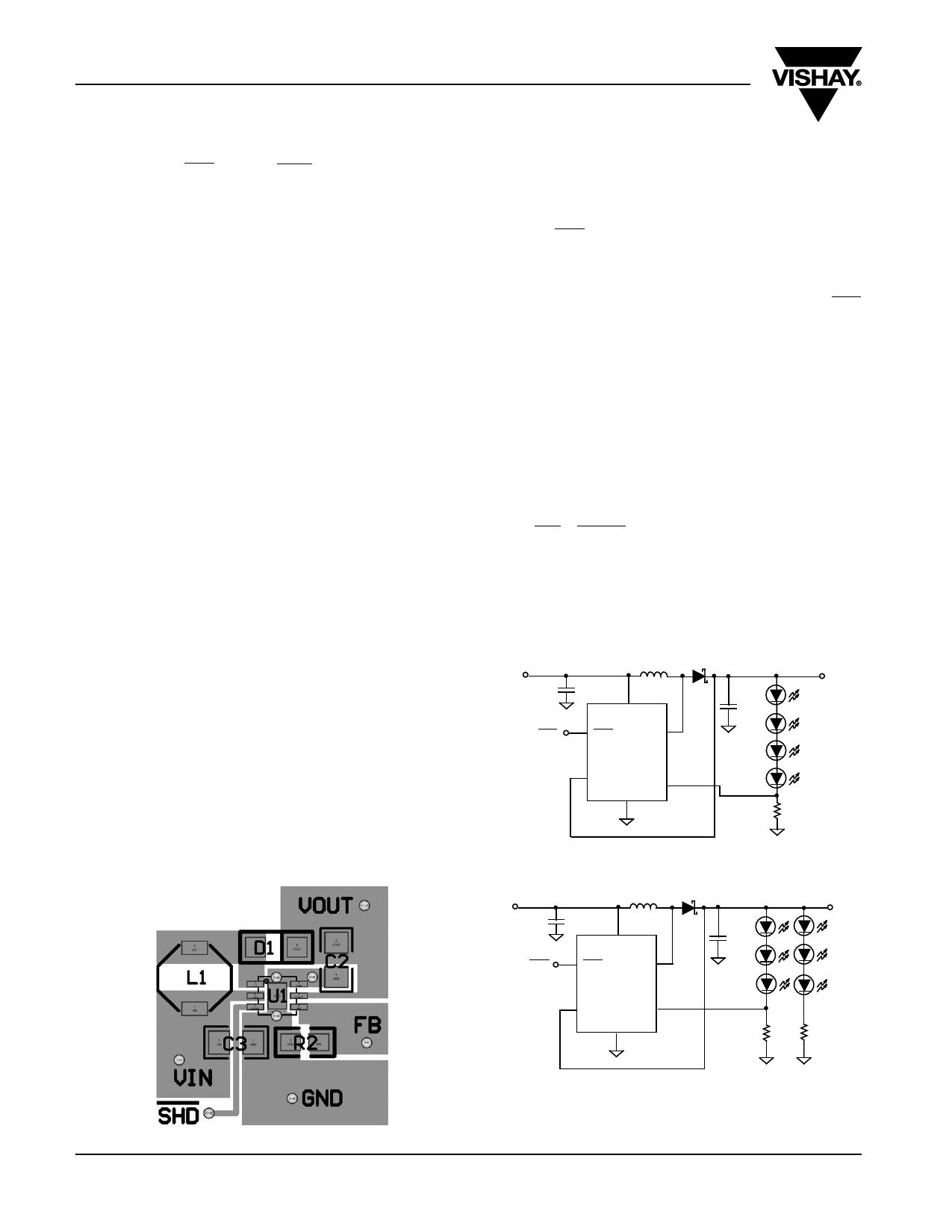
As shown in Figures 6 and 7, the SiP12506 can be used to
drive four LEDs in series or to drive parallel strings of LEDs.
VIN
1 µF
SHD
MBR0530
L
2 10 µH
VIN
3 SHD
1
LX
COUT
1 µF
SiP12506
5 VOUT
FB 4
GND
6
0. 208 V
10.5 Ω
VOUT
Figure 6. SiP12506 Driving Four LEDs
MBR0530
VIN
1 µF
L
2 10 µH
SHD
VIN
3 SHD
1
LX
COUT
1 µF
SiP12506
5 VOUT
4
FB
GND
6
0. 208 V
10.5 Ω 10.5 Ω
VOUT
Figure 7. SiP12506 Driving Six LEDs
www.vishay.com
8
Figure 5.
Document Number: 73861
S-70547–Rev. D, 26-Mar-07
Share Link: 