CA3162 データシートの表示(PDF) - Harris Semiconductor
部品番号
コンポーネント説明
メーカー
CA3162 Datasheet PDF : 7 Pages
| |||
CA3162, CA3162A
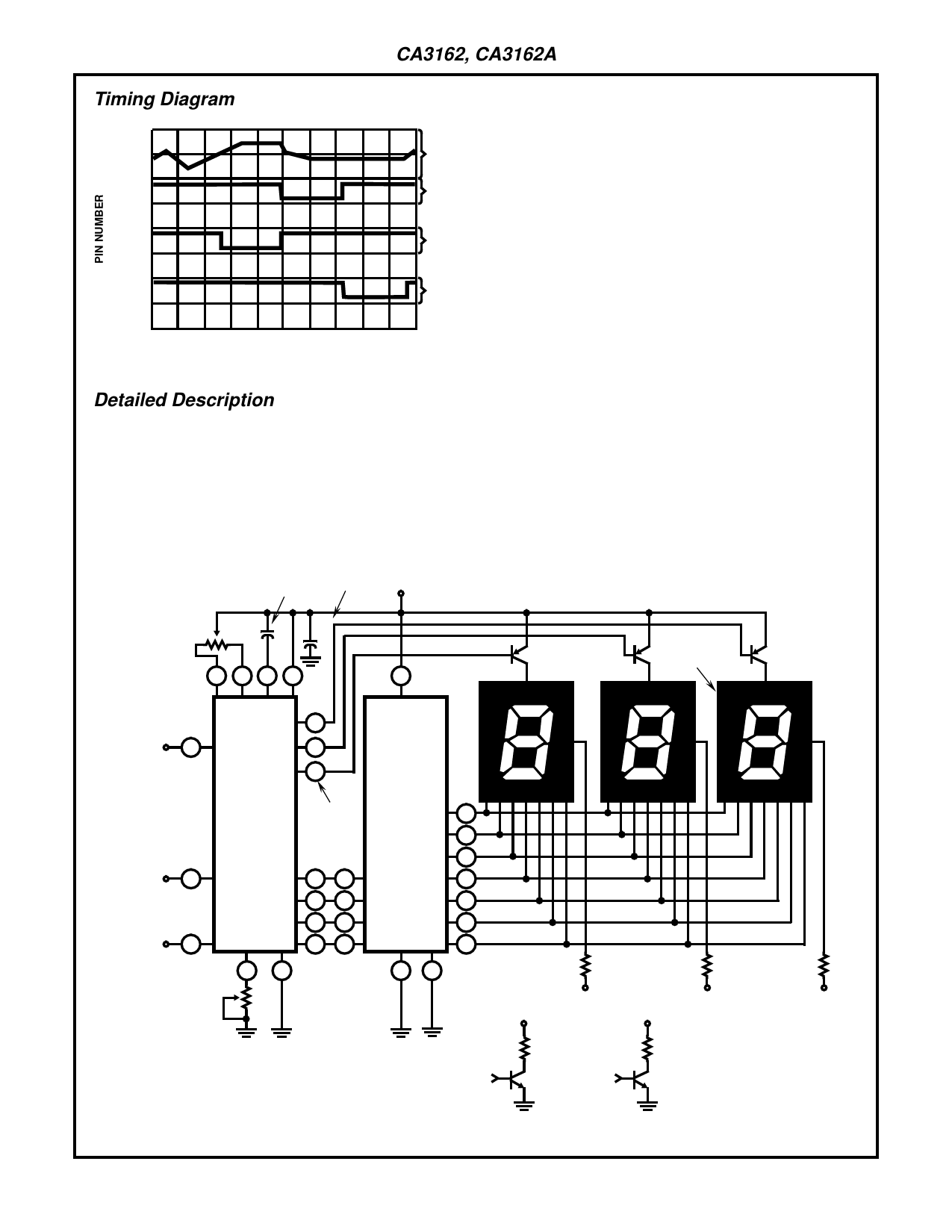
Timing Diagram
12
5 (LSD)
4 (MSD)
3 (NSD)
200mV
500mV
500mV
500mV
2ms/DIVISION
FIGURE 1. HIGH SPEED MODE
Detailed Description
The Functional Block Diagram of the CA3162E shows the V/I
converter and reference current generator, which is the heart
of the system. The V/I converter converts the input voltage
applied between pins 10 and 11 to a current that charges the
integrating capacitor on pin 12 for a predetermined time inter-
val. At the end of the charging interval, the V/I converter is dis-
connected from the integrating capacitor, and a band gap
reference constant current source of opposite polarity is con-
nected. The number of clock counts that elapse before the
charge is restored to its original value is a direct measure of
the signal induced current. The restoration is sensed by the
comparator, which in turn latches the counter. The count is
then multiplexed to the BCD outputs.
The timing for the CA3162E is supplied by a 786Hz ring oscil-
lator, and the input at pin 6 determines the sampling rate. A
5V input provides a high speed sampling rate (96Hz), and
grounding or floating pin 6 provides a low speed (4Hz) sam-
pling rate. When pin 6 is fixed at +1.2V (by placing a 12K
resistor between pin 6 and the +5V supply) a “hold” feature is
available. While the CA3162E is in the hold mode, sampling
continues at 4Hz but the display data are latched to the last
reading prior to the application of the 1.2V. Removal of the
1.2V restores continuous display changes. Note, however,
that the sampling rate remains at 4Hz.
Figure 1 shows the timing of sampling and digit select pulses
for the high speed mode. Note that the basic A/D conversion
process requires approximately 5ms in both modes.
The “EEE” or “---” displays indicate that the range of the sys-
tem has been exceeded in the positive or negative direction,
respectively. Negative voltages to -99mV are displayed with
the minus sign in the MSD. The BCD code is 1010 for a nega-
tive overrange (---) and 1011 for a positive overrange (EEE).
NOTE 1 NOTE 2
+5V
0.27µF
0.1
µF
NORMAL
16 16 16 16
LOW SPEED MODE:
V6 = GROUND OR
OPEN
5
HOLD:
V6 = 1.2V
6
3
4
HIGH SPEED MODE:
V6 = 5V
CA3162E
DIGIT
DRIVERS
11
HIGH
INPUTS
LOW
10
BCD
OUTPUTS
16 6
15 2
11
27
GAIN
ADJ
13 7
10
kΩ
16
MSD
a
fb
g
ec
d
13
CA3161E
12
11
10
9
15
14
83
CA3162E
PINS
3, 4, 5
NSD
COMMON
ANODE LED
DISPLAYS
LSD
POWER
2N2907, 2N3906
OR EQUIV.
a
fb
g
ec
d
a
fb
g
ec
d
R1
150Ω
CA3162E
PINS
1, 2, 15, 16
R2
150Ω
R3
150Ω
NOTES:
1. The capacitor used here must be a low dielectric absorption type
such as a polyester or polystyrene type.
2. This capacitor should be placed as close as possible to the power
and ground Pins of the CA3161E.
1kΩ
DIGIT
DRIVER
75Ω
BCD SEGMENT
DRIVERS
FIGURE 2. BASIC DIGITAL READOUT SYSTEM USING THE CA3162E AND THE CA3161E
2-8
Share Link: 