SMAJ54 データシートの表示(PDF) - Daesan Electronics Corp.
部品番号
コンポーネント説明
メーカー
SMAJ54 Datasheet PDF : 4 Pages
| |||
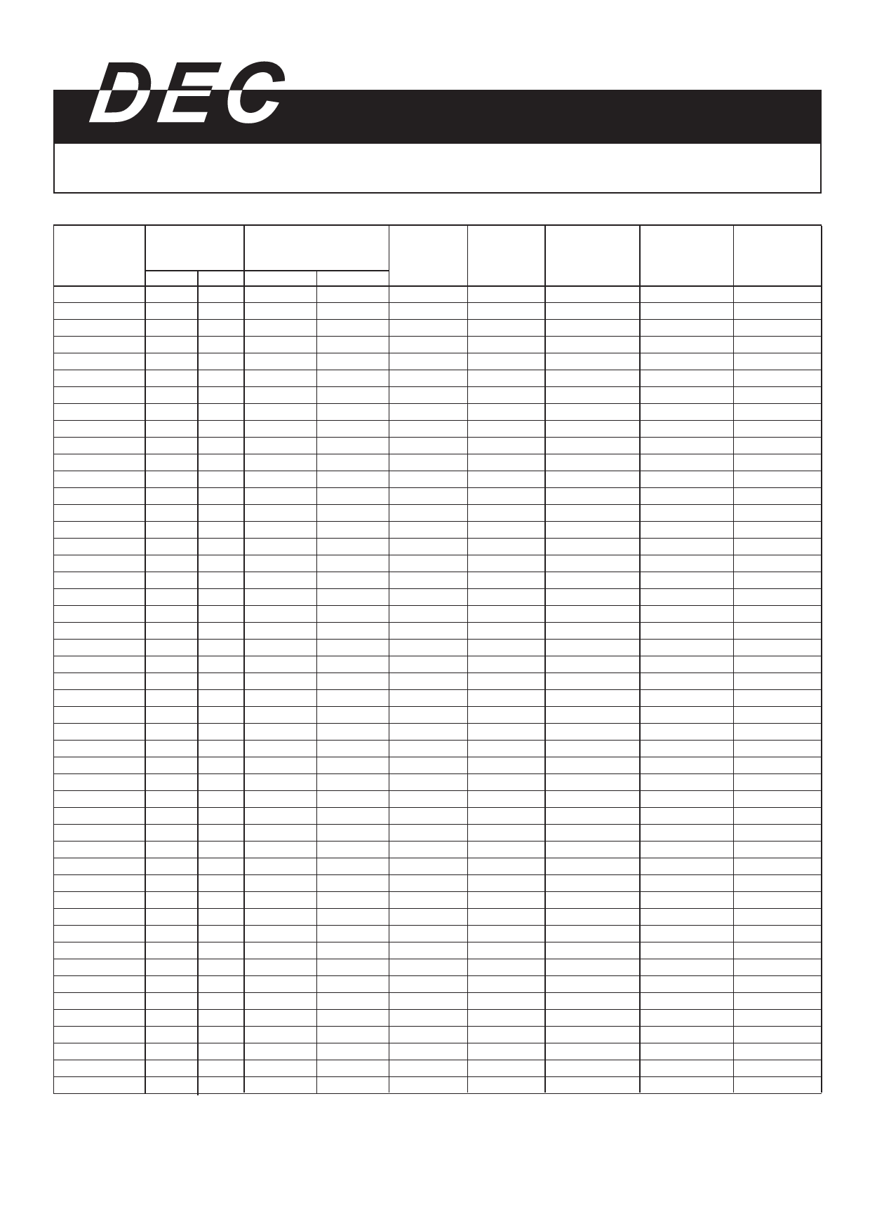
ELECTRICAL CHARACTERISTIC
Ratings at 25℃ ambient temperature unless otherwise specified. VF=3.5V at IF=25A (uni-directional only)
Device Type
S MAJ 33(C)
S MAJ 33(C)A
S MAJ 36(C)
S MAJ 36(C)A
S MAJ 40(C)
S MAJ 40(C)A
S MAJ 43(C)
S MAJ 43(C)A
S MAJ 45(C)
S MAJ 45(C)A
S MAJ 48(C)
S MAJ 48(C)A
S MAJ 51(C)
S MAJ 51(C)A
S MAJ 54(C)
S MAJ 54(C)A
S MAJ 58(C)
S MAJ 58(C)A
S MAJ 60(C)
S MAJ 60(C)A
S MAJ 64(C)
S MAJ 64(C)A
S MAJ 70(C)
S MAJ 70(C)A
S MAJ 75(C)
S MAJ 75(C)A
S MAJ 78(C)
S MAJ 78(C)A
S MAJ 85(C)
S MAJ 85(C)A
S MAJ 90(C)
S MAJ 90(C)A
S MAJ 100(C)
S MAJ 100(C)A
S MAJ 110(C)
S MAJ 110(C)A
S MAJ 120(C)
S MAJ 120(C)A
S MAJ 130(C)
S MAJ 130(C)A
S MAJ 150(C)
S MAJ 150(C)A
S MAJ 160(C)
S MAJ 160(C)A
S MAJ 170(C)
S MAJ 170(C)A
S MAJ 188(C)
S MAJ 188(C)A
Device
Marking
Code
UNI
BI
CL
YL
CM YM
CN YN
CP
YP
CQ YQ
CR
YR
CS
YS
CT
YT
CU
YU
CV
YV
CW YW
CX
YX
CY
YY
CZ
YZ
RD
ZD
RE
ZE
RF
ZF
RG
ZG
RH
ZH
RK
ZK
RL
ZL
R M ZM
RN
ZN
RP
ZP
R Q ZQ
RR
ZR
RS
ZS
RT
ZT
RU
ZU
RV
ZV
RW ZW
RX
ZX
RY
ZY
RZ
ZZ
VD
VD
SE
VE
SF
VF
VG
VG
SH
VH
VK
VK
SL
VL
VM VM
SN
VN
SP
VP
SQ
VQ
SR
VR
ST
VT
SS
VS
Breakdown Voltage
V(BR) at I T (1)
(V)
Min
Max
36.7
44.9
36.7
40.6
40.0
48.9
40.0
44.2
44.4
54.3
44.4
49.1
47.8
58.4
47.8
52.8
50.0
61.1
50.0
55.3
53.3
65.1
53.3
58.9
56.7
69.3
56.7
62.7
60.0
73.3
60.0
66.3
64.4
78.7
64.4
71.2
66.7
81.5
66.7
73.7
71.1
86.9
71.1
78.6
77.8
95.1
77.8
86.0
83.3
102
83.3
92.1
86.7
106
86.7
95.8
94.4
115
94.4
104
100
122
100
111
111
136
111
123
122
149
122
135
133
163
133
147
144
176
144
159
167
204
167
185
178
218
178
197
189
231
189
209
209
255
209
231
Test
Current
IT (mA)
1.0
1.0
1.0
1.0
1.0
1.0
1.0
1.0
1.0
1.0
1.0
1.0
1.0
1.0
1.0
1.0
1.0
1.0
1.0
1.0
1.0
1.0
1.0
1.0
1.0
1.0
1.0
1.0
1.0
1.0
1.0
1.0
1.0
1.0
1.0
1.0
1.0
1.0
1.0
1.0
1.0
1.0
1.0
1.0
1.0
1.0
1.0
1.0
Stand-off
Voltage
VWM (V)
33
33
36
36
40
40
43
43
45
45
48
48
51
51
54
54
58
58
60
60
64
64
70
70
75
75
78
78
85
85
90
90
100
100
110
110
120
120
130
130
150
150
160
160
170
170
188
188
Maximum
Maximum
Maximum
Reverse Leakage Peak Pulse Surge Clamping
at VWM
ID (μA) (3)
Current I PPM Voltage at IPPM
(A)(2)
VC (V)
1.0
6.8
59.0
1.0
7.5
53.3
1.0
6.2
64.3
1.0
6.9
58.1
1.0
5.6
71.4
1.0
6.2
64.5
1.0
5.2
76.7
1.0
5.8
69.4
1.0
5.0
80.3
1.0
5.5
72.7
1.0
4.7
85.5
1.0
5.2
77.4
1.0
4.4
91.1
1.0
4.9
82.4
1.0
4.2
96.3
1.0
4.6
87.1
1.0
3.9
103
1.0
4.3
93.6
1.0
3.7
107
1.0
4.1
96.8
1.0
3.5
114
1.0
3.9
103
1.0
3.2
125
1.0
3.5
113
1.0
3.0
134
1.0
3.3
121
1.0
2.9
139
1.0
3.2
126
1.0
2.0
151
1.0
2.2
137
1.0
1.9
160
1.0
2.1
146
1.0
1.7
179
1.0
1.9
162
1.0
1.5
196
1.0
1.7
177
1.0
1.4
214
1.0
1.6
193
1.0
1.3
231
1.0
1.4
209
1.0
1.1
268
1.0
1.2
243
1.0
1.0
287
1.0
1.2
259
1.0
0.99
304
1.0
1.09
275
1.0
0.9
344
1.0
0.91
328
Notes : (1) P uls e tes t: tp =50ms
(2) S urge current waveform per F ig. 3 and derate per F ig. 2
(3) For bi-directional types having V WM of 10 V olts and les s, the ID limit is doubled
(4) All terms and s ymbols are cons is tent with ANS I/IE E E C 62.35
Share Link: 