SMF05T1G データシートの表示(PDF) - ON Semiconductor
部品番号
コンポーネント説明
メーカー
SMF05T1G Datasheet PDF : 5 Pages
| |||
SMF05
MAXIMUM RATINGS (TA = 25°C unless otherwise noted)
Characteristic
Symbol
Value
Unit
Peak Power Dissipation @ 8 X 20 ms @TA ≤ 25°C (Note 1)
Ppk
200
W
Maximum Junction Temperature
TJmax
150
°C
Operating Junction and Storage Temperature Range
TJ, Tstg
−55 to +150
°C
ESD Discharge
IEC61000−4−2, Air Discharge
VPP
IEC61000−4−2, Contact Discharge
16
kV
9
Lead Solder Temperature (10 seconds duration)
TL
260
°C
Stresses exceeding those listed in the Maximum Ratings table may damage the device. If any of these limits are exceeded, device functionality
should not be assumed, damage may occur and reliability may be affected.
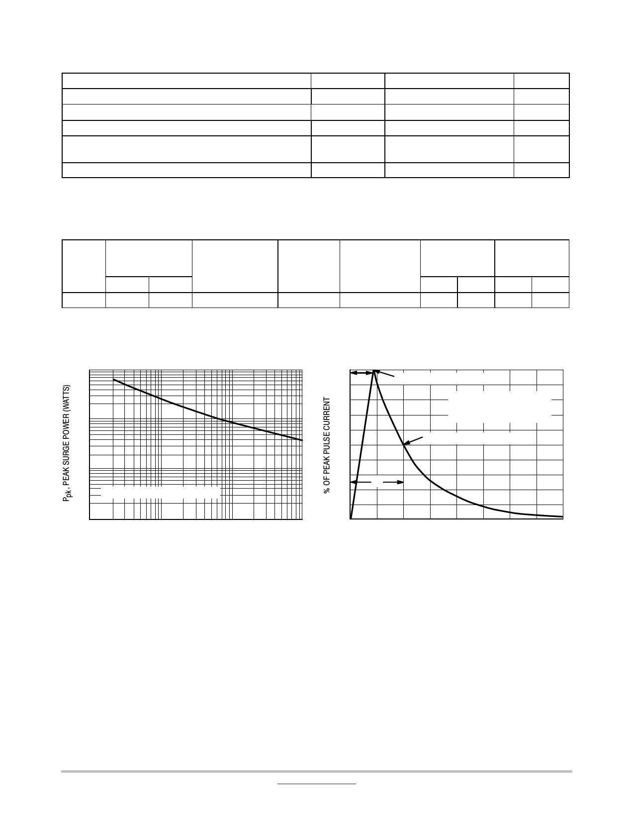
1. Non−repetitive current per Figure 2. Derate per Figure 3.
ELECTRICAL CHARACTERISTICS (TA = 25°C unless otherwise noted)
Device
SMF05
Breakdown Voltage
VBR @ 1 mA (Volts)
Min
Max
6.0
7.2
Leakage Current
IR @ VRWM = 5 V
(mA)
5.0
Capacitance
@ 0 V Bias
(pF)
90
Max
VF @ IF = 200 mA
(V)
1.25
Max Clamping
Voltage (VC)
@ IPP
IPP (A) VC (V)
1.0
9.5
Max Clamping
Voltage (VC)
@ IPP
IPP (A) VC (V)
12
12.5
TYPICAL PERFORMANCE CURVES
(TA = 25°C unless otherwise noted)
1000
100
10
NOTE: Non−Repetitive Surge.
1
1
10
100
1000
t, TIME (ms)
Figure 1. Peak Power Dissipation versus
Pulse Width
100
tr
90
80
70
60
50
PEAK VALUE IRSM @ 8 ms
PULSE WIDTH (tP) IS DEFINED
AS THAT POINT WHERE THE
PEAK CURRENT DECAY = 8 ms
HALF VALUE IRSM/2 @ 20 ms
40
30
tP
20
10
0
0
20
40
60
80
t, TIME (ms)
Figure 2. Pulse Waveform 8 x 20 ms
www.onsemi.com
2
Share Link: 