SN74LS298D データシートの表示(PDF) - ON Semiconductor
部品番号
コンポーネント説明
メーカー
SN74LS298D Datasheet PDF : 8 Pages
| |||
SN74LS298
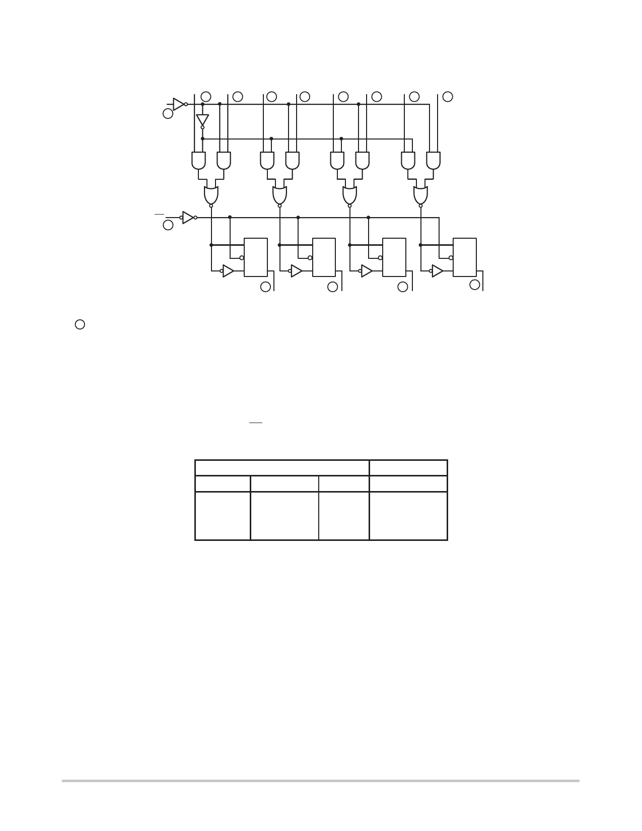
LOGIC OR BLOCK DIAGRAM
I1a
I0a
I1b
I0b
2
3
1
4
S
10
I1c
5
I0c
9
I1d
6
I0d
7
CP
11
VCC = PIN 16
GND = PIN 8
= PIN NUMBERS
R
CP
S Qa
15
Qa
R
CP
S Qb
14
Qb
R
CP
S Qc
13
Qc
R
CP
S Qd
12
Qd
FUNCTIONAL DESCRIPTION
The LS298 is a high speed Quad 2-Port Register. It selects
four bits of data from two sources (ports)under the control
of a Common Select Input (S). The selected data is
transferred to the 4-bit output register synchronous with the
HIGH to LOW transition of the Clock input (CP). The 4-bit
output register is fully edge-triggered. The Data inputs (I)
and Select input (S) must be stable only one setup time prior
to the HIGH to LOW transition of the clock for predictable
operation.
TRUTH TABLE
INPUTS
OUTPUT
S
I0
I1
Q
I
I
X
L
I
h
X
H
h
X
I
L
h
X
h
H
L = LOW Voltage Level
H = HIGH Voltage Level
X = Don’t Care
I = LOW Voltage Level one setup time prior to the HIGH to LOW clock transition.
h = HIGH Voltage Level one setup time prior to the HIGH to LOW clock transition.
http://onsemi.com
3
Share Link: 