SPU01N60C3 データシートの表示(PDF) - Infineon Technologies
部品番号
コンポーネント説明
メーカー
SPU01N60C3 Datasheet PDF : 11 Pages
| |||
SPU01N60C3
SPD01N60C3
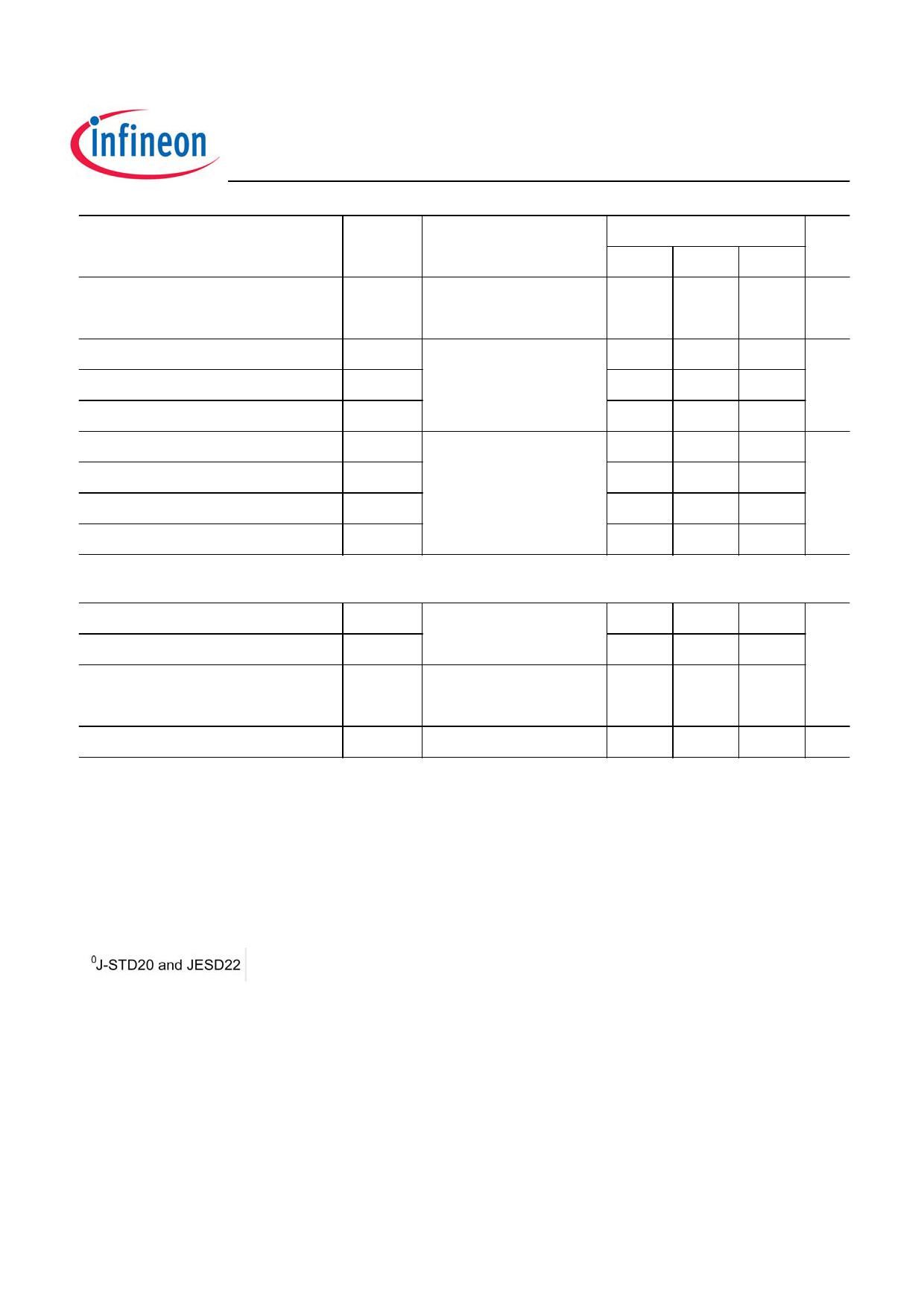
Electrical Characteristics , at Tj = 25 °C, unless otherwise specified
Parameter
Symbol
Conditions
Values
Unit
min. typ. max.
Transconductance
gfs
VDS≥2*ID*RDS(on)max,
- 0.75 - S
ID=0.5A
Input capacitance
Ciss
VGS=0V, VDS=25V,
-
Output capacitance
Coss
f=1MHz
-
Reverse transfer capacitance Crss
-
Turn-on delay time
td(on)
VDD=350V, VGS=0/10V,
-
Rise time
tr
ID=0.8A, RG=100Ω
-
Turn-off delay time
td(off)
-
100 - pF
40
-
2.5
-
30
- ns
25
-
55 82
Fall time
tf
-
30 45
Gate Charge Characteristics
Gate to source charge
Gate to drain charge
Qgs
Qgd
VDD=350V, ID=0.8A
Gate charge total
Qg
VDD=350V, ID=0.8A,
VGS=0 to 10V
Gate plateau voltage
V(plateau) VDD=350V, ID=0.8A
-
0.9
- nC
-
2.2
-
-
3.9
5
-
5.5
-V
1Repetitve avalanche causes additional power losses that can be calculated asPAV=EAR*f.
2Device on 40mm*40mm*1.5mm epoxy PCB FR4 with 6cm² (one layer, 70 µm thick) copper area for drain
connection. PCB is vertical without blown air.
3ISD<=ID, di/dt<=400A/us, VDClink=400V, Vpeak<VBR, DSS, Tj<Tj,max.
Identical low-side and high-side switch.
Rev. 2.5
Page 3
2008-04-07
Share Link: 