SST39SF010A-45-4C-U1 データシートの表示(PDF) - Silicon Storage Technology
部品番号
コンポーネント説明
メーカー
SST39SF010A-45-4C-U1 Datasheet PDF : 22 Pages
| |||
1 Mbit / 2 Mbit / 4 Mbit Multi-Purpose Flash
SST39SF010A / SST39SF020A / SST39SF040
Preliminary Specification
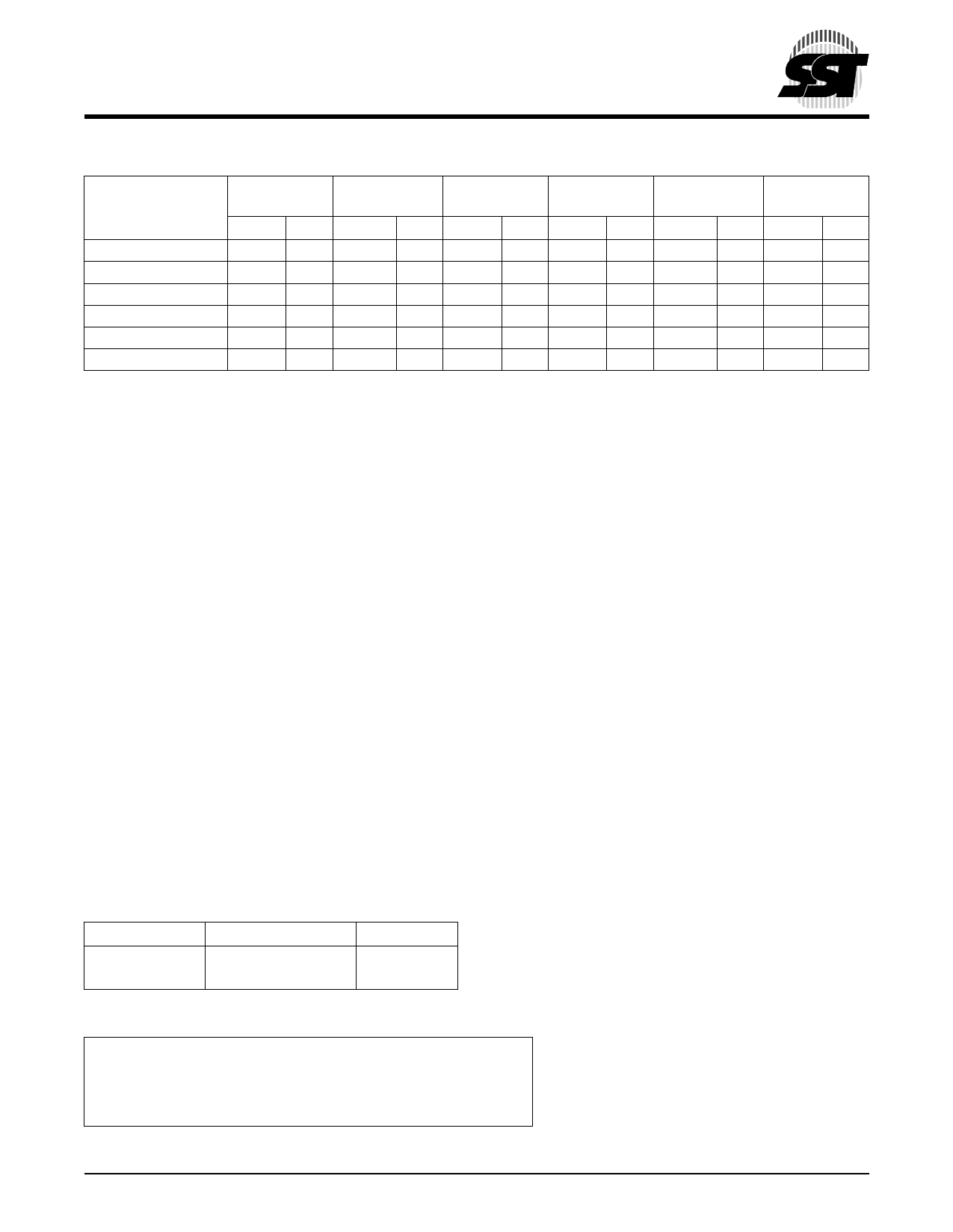
TABLE 4: SOFTWARE COMMAND SEQUENCE
Command
Sequence
1st Bus
Write Cycle
2nd Bus
Write Cycle
3rd Bus
Write Cycle
4th Bus
Write Cycle
5th Bus
Write Cycle
6th Bus
Write Cycle
Addr1 Data Addr1 Data Addr1 Data Addr1 Data Addr1 Data Addr1 Data
Byte-Program
5555H AAH 2AAAH 55H 5555H A0H BA2 Data
Sector-Erase
Chip-Erase
5555H AAH 2AAAH 55H 5555H 80H 5555H AAH 2AAAH 55H SAX3 30H
5555H AAH 2AAAH 55H 5555H 80H 5555H AAH 2AAAH 55H 5555H 10H
Software ID Entry4,5 5555H AAH 2AAAH 55H 5555H 90H
Software ID Exit6
XXH F0H
Software ID Exit6
5555H AAH 2AAAH 55H 5555H F0H
1. Address format A14-A0 (Hex), Addresses A15 - AMS can be VIL or VIH, but no other value, for the Command sequence.
2. BA = Program Byte address
3. SAX for Sector-Erase; uses AMS-A12 address lines
AMS = Most significant address
AMS = A16 for SST39SF010A, A17 for SST39SF020A, and A18 for SST39SF040
4. The device does not remain in Software Product ID Mode if powered down.
5. With AMS-A1 =0; SST Manufacturer’s ID= BFH, is read with A0 = 0,
SST39SF010A Device ID = B5H, is read with A0 = 1
SST39SF020A Device ID = B6H, is read with A0 = 1
SST39SF040 Device ID = B7H, is read with A0 = 1
6. Both Software ID Exit operations are equivalent
T4.2 398
Absolute Maximum Stress Ratings (Applied conditions greater than those listed under “Absolute Maximum
Stress Ratings” may cause permanent damage to the device. This is a stress rating only and functional operation
of the device at these conditions or conditions greater than those defined in the operational sections of this data
sheet is not implied. Exposure to absolute maximum stress rating conditions may affect device reliability.)
Temperature Under Bias . . . . . . . . . . . . . . . . . . . . . . . . . . . . . . . . . . . . . . . . . . . . . . . . . . . . . . . . . -55°C to +125°C
Storage Temperature . . . . . . . . . . . . . . . . . . . . . . . . . . . . . . . . . . . . . . . . . . . . . . . . . . . . . . . . . . . -65°C to +150°C
D. C. Voltage on Any Pin to Ground Potential . . . . . . . . . . . . . . . . . . . . . . . . . . . . . . . . . . . . . . . -0.5V to VDD + 0.5V
Transient Voltage (<20 ns) on Any Pin to Ground Potential . . . . . . . . . . . . . . . . . . . . . . . . . . . . -1.0V to VDD + 1.0V
Voltage on A9 Pin to Ground Potential . . . . . . . . . . . . . . . . . . . . . . . . . . . . . . . . . . . . . . . . . . . . . . . . -0.5V to 13.2V
Package Power Dissipation Capability (Ta = 25°C) . . . . . . . . . . . . . . . . . . . . . . . . . . . . . . . . . . . . . . . . . . . . . . 1.0W
Through Hold Lead Soldering Temperature (10 Seconds) . . . . . . . . . . . . . . . . . . . . . . . . . . . . . . . . . . . . . . . 300°C
Surface Mount Lead Soldering Temperature (3 Seconds) . . . . . . . . . . . . . . . . . . . . . . . . . . . . . . . . . . . . . . . 240°C
Output Short Circuit Current1 . . . . . . . . . . . . . . . . . . . . . . . . . . . . . . . . . . . . . . . . . . . . . . . . . . . . . . . . . . . . 100 mA
1. Outputs shorted for no more than one second. No more than one output shorted at a time.
OPERATING RANGE
Range
Commercial
Industrial
Ambient Temp
0°C to +70°C
-40°C to +85°C
VDD
5.0V±10%
5.0V±10%
AC CONDITIONS OF TEST
Input Rise/Fall Time . . . . . . . . . . . . . . 5 ns
Output Load . . . . . . . . . . . . . . . . . . . . . CL = 30 pF for 45 ns
Output Load . . . . . . . . . . . . . . . . . . . . . CL = 100 pF for 70 ns
See Figures 13 and 14
©2001 Silicon Storage Technology, Inc.
7
S71147-02-000 5/01 398
Share Link: 