SST39VF1601-70-4C-B3K データシートの表示(PDF) - Silicon Storage Technology
部品番号
コンポーネント説明
メーカー
SST39VF1601-70-4C-B3K
Silicon Storage Technology

SST39VF1601-70-4C-B3K Datasheet PDF : 32 Pages
| |||
16 Mbit / 32 Mbit / 64 Mbit Multi-Purpose Flash Plus
SST39VF1601 / SST39VF3201 / SST39VF6401
SST39VF1602 / SST39VF3202 / SST39VF6402
Preliminary Specifications
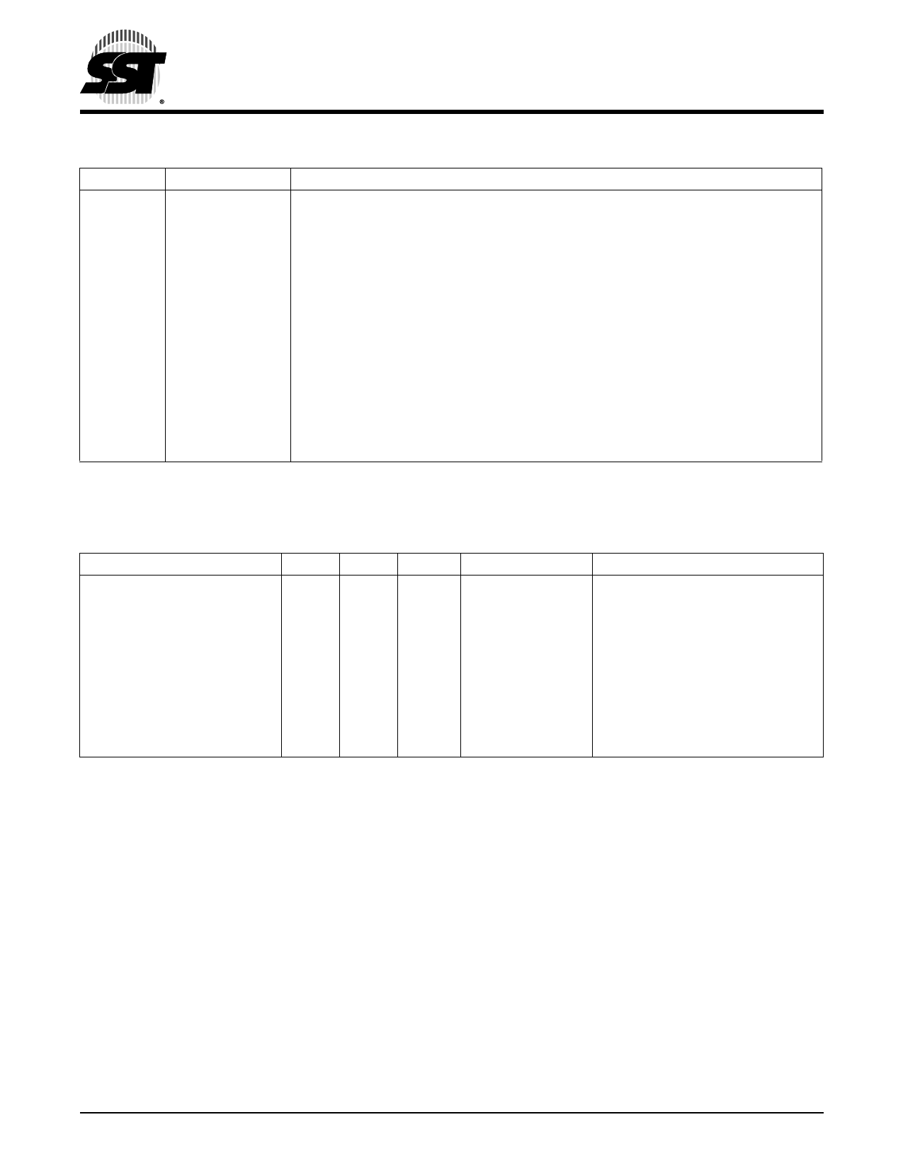
TABLE 4: PIN DESCRIPTION
Symbol
Pin Name
Functions
AMS1-A0
DQ15-DQ0
Address Inputs
Data Input/output
To provide memory addresses.
During Sector-Erase AMS-A11 address lines will select the sector.
During Block-Erase AMS-A15 address lines will select the block.
To output data during Read cycles and receive input data during Write cycles.
Data is internally latched during a Write cycle.
The outputs are in tri-state when OE# or CE# is high.
WP#
Write Protect
To protect the top/bottom boot block from Erase/Program operation when grounded.
RST#
Reset
To reset and return the device to Read mode.
CE#
Chip Enable
To activate the device when CE# is low.
OE#
Output Enable
To gate the data output buffers.
WE#
Write Enable
To control the Write operations.
VDD
Power Supply
To provide power supply voltage: 2.7-3.6V
VSS
Ground
NC
No Connection
Unconnected pins.
1. AMS = Most significant address
AMS = A19 for SST39VF1601/1602, A20 for SST39VF3201/3202, and A21 for SST39VF6401/6402
T4.2 1223
TABLE 5: OPERATION MODES SELECTION
Mode
Read
Program
Erase
CE#
VIL
VIL
VIL
OE#
VIL
VIH
VIH
Standby
Write Inhibit
Product Identification
Software Mode
VIH
X
X
VIL
X
X
VIL
VIL
1. X can be VIL or VIH, but no other value.
WE#
VIH
VIL
VIL
DQ
DOUT
DIN
X1
X High Z
X
High Z/ DOUT
VIH High Z/ DOUT
VIH
Address
AIN
AIN
Sector or block address,
XXH for Chip-Erase
X
X
X
See Table 6
T5.0 1223
©2003 Silicon Storage Technology, Inc.
8
S71223-03-000
11/03
Share Link: